Original Link: https://www.anandtech.com/show/11185/nvidia-announces-jetson-tx2-parker
NVIDIA Announces Jetson TX2: Parker Comes To NVIDIA’s Embedded System Kit
by Ryan Smith on March 7, 2017 9:00 PM EST- Posted in
- SoCs
- NVIDIA
- Tegra
- Machine Learning
- Tegra Parker
- Jetson
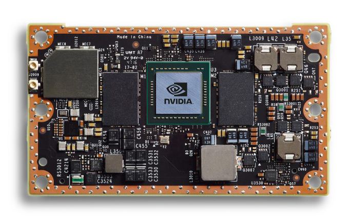
For a few years now, NVIDIA has been offering their line of Jetson embedded system kits. Originally launched using Tegra K1 in 2014, the first Jetson was designed to be a dev kit for groups looking to build their own Tegra-based devices from scratch. Instead, what NVIDIA surprisingly found, was that groups would use the Jetson board as-is instead and build their devices around that. This unexpected market led NVIDIA to pivot a bit on what Jetson would be, resulting in the second-generation Jetson TX1, a proper embedded system board that can be used for both development purposes and production devices.
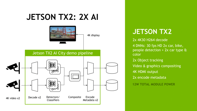
This relaunched Jetson came at an interesting time for NVIDIA, which was right when their fortunes in neural networking/deep learning took off in earnest. Though the Jetson TX1 and underlying Tegra X1 SoC lack the power needed for high-performance use cases – these are after all based on an SoC designed for mobile applications – they have enough power for lower-performance inferencing. As a result, the Jetson TX1 has become an important part of NVIDIA’s neural networking triad, offering their GPU architecture and its various benefits for devices doing inferencing at the “edge” of a system.
Now about a year and a half after the launch of the Jetson TX1, NVIDIA is going to be giving the Jetson platform a significant update in the form of the Jetson TX2. This updated Jetson is not as radical a change as the TX1 before it was – NVIDIA seems to have found a good place in terms of form factor and the platform’s core feature set – but NVIDIA is looking to take what worked with TX1 and further ramp up the performance of the platform.
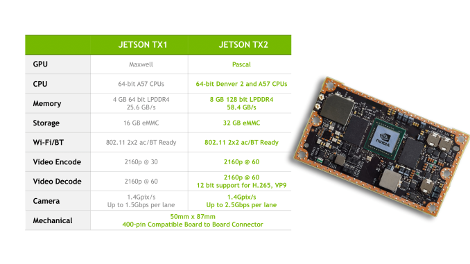
The big change here is the upgrade to NVIDIA’s newest-generation Parker SoC. While Parker never made it into third-party mobile designs, NVIDIA has been leveraging it internally for the Drive system and other projects, and now it will finally become the heart of the Jetson platform as well. Relative to the Tegra X1 in the previous Jetson, Parker is a bigger and better version of the SoC. The GPU architecture is upgraded to NVIDIA’s latest-generation Pascal architecture, and on the CPU side NVIDIA adds a pair of Denver 2 CPU cores to the existing quad-core Cortex-A57 cluster. Equally important, Parker finally goes back to a 128-bit memory bus, greatly boosting the memory bandwidth available to the SoC. The resulting SoC is fabbed on TSMC’s 16nm FinFET process, giving NVIDIA a much-welcomed improvement in power efficiency.
Paired with Parker on the Jetson TX2 as supporting hardware is 8GB of LPDDR4-3733 DRAM, a 32GB eMMC flash module, a 2x2 802.11ac + Bluetooth wireless radio, and a Gigabit Ethernet controller. The resulting board is still 50mm x 87mm in size, with NVIDIA intending it to be drop-in compatible with Jetson TX1.
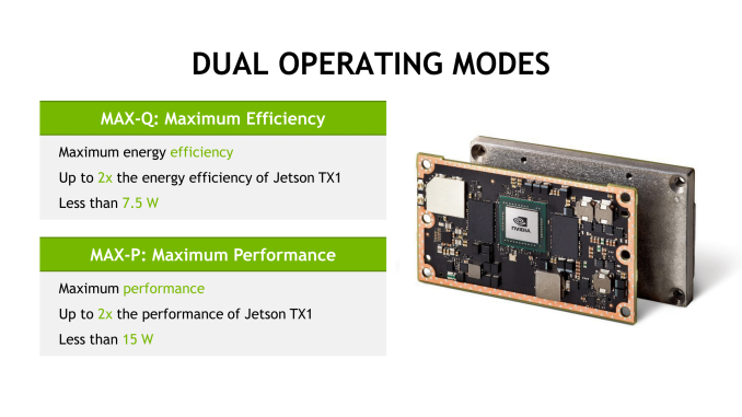
Given these upgrades to the core hardware, unsurprisingly NVIDIA’s primary marketing angle with the Jetson TX2 is on its performance relative to the TX1. In a bit of a departure from the TX1, NVIDIA is canonizing two performance modes on the TX2: Max-Q and Max-P. Max-Q is the company’s name for TX2’s energy efficiency mode; at 7.5W, this mode clocks the Parker SoC for efficiency over performance – essentially placing it right before the bend in the power/performance curve – with NVIDIA claiming that this mode offers 2x the energy efficiency of the Jetson TX1. In this mode, TX2 should have similar performance to TX1 in the latter's max performance mode.
Meanwhile the board’s Max-P mode is its maximum performance mode. In this mode NVIDIA sets the board TDP to 15W, allowing the TX2 to hit higher performance at the cost of some energy efficiency. NVIDIA claims that Max-P offers up to 2x the performance of the Jetson TX1, though as GPU clockspeeds aren't double TX1's, it's going to be a bit more sensitive on an application-by-application basis.
| NVIDIA Jetson TX2 Performance Modes | |||||
| Max-Q | Max-P | Max Clocks | |||
| GPU Frequency | 854MHz | 1122MHz | 1302MHz | ||
| Cortex-A57 Frequency | 1.2GHz | Stand-Alone: 2GHz w/Denver: 1.4GHz |
2GHz+ | ||
| Denver 2 Frequency | N/A | Stand-Alone: 2GHz w/A57: 1.4GHz |
2GHz | ||
| TDP | 7.5W | 15W | N/A | ||
In terms of clockspeeds, NVIDIA has disclosed that in Max-Q mode, the GPU is clocked at 854MHz while the Cortex-A57 cluster is at 1.2GHz. Going to Max-P increases the GPU clockspeed further to 1122MHz, and allows for multiple CPU options; either the Cortex-A57 cluster or Denver 2 cluster can be run at 2GHz, or both can be run at 1.4GHz. Though when it comes to all-out performance, even Max-P mode is below the TX2's limits; the GPU clock can top out at just over 1300MHz and CPU clocks can reach 2GHz or better. Power states are configurable, so customers can dial in the TDPs and desired clockspeeds they want, however NVIDIA notes that using the maximum clocks goes further outside of the Parker SoC’s efficiency range.
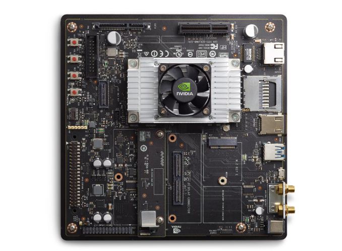
Finally, along with announcing the Jetson TX2 module itself, NVIDIA is also announcing a Jetson TX2 development kit. The dev kit will actually ship first – it ships next week in the US and Europe, with other regions in April – and contains a TX2 module along with a carrier board to provide I/O breakout and interfaces to various features such as the USB, HDMI, and Ethernet. Judging from the pictures NVIDIA has sent over, the TX2 carrier board is very similar (if not identical) to the TX1 carrier board, so like the TX2 itself is should be familiar to existing Jetson developers.
With the dev kit leading the charge for Jetson TX2, NVIDIA will be selling it for $599 retail/$299 education, the same price the Jetson TX1 dev kit launched at back in 2015. Meanwhile the stand-alone Jetson TX2 module will be arriving in Q2’17, priced at $399 in 1K unit quantities. In the case of the module, this means prices have gone up a bit since the last generation; the TX2 is hitting the market at $100 higher than where the TX1 launched.
Source: NVIDIA

