Original Link: https://www.anandtech.com/show/945
It was the summer of 2001, Computex was heating up (both literally and figuratively) and NVIDIA took the world by storm with the launch of their nForce chipset. Our contacts at VIA were sweating nervously as they faced new pressures from not only SiS but now the biggest name in graphics. Having seen what NVIDIA did to 3dfx, VIA’s concerns were understandable; especially considering the incredible amount of hype that was drummed up around the launch of the original nForce.
As they always say, hindsight is 20-20 and you all now know that the launch of NVIDIA’s first chipset wasn’t flawless. It was no less than 3 months after the launch of the chipset at Computex that we saw our first reference board from NVIDIA; it was a matter of several weeks after that before third party boards started appearing on the market, and at extremely high prices. Because of this large gap between the announcement and the shipping date for motherboards, it has only been recently that NVIDIA has garnered any significant OEM design wins based on their nForce chipset.
Because of everything that happened with the original nForce launch, we were quite skeptical when we heard that NVIDIA would be showing off nForce2 at Computex this year. However when we arrived in the humid city of Taipei we caught wind of NVIDIA’s slight change in nForce2 launch strategy; motherboard manufacturers were able to show off all of their nForce2 solutions (and even their CK8 Hammer chipset) but NVIDIA didn’t publicly disclose any details about the chipset. Instead, we were given a look at nForce2 behind closed doors and told not to speak about the specifics until now.
 Today
we’re finally able to tell you all about NVIDIA’s second try at
an Athlon chipset – nForce2. But before you get too excited, it will still
be a matter of weeks before we can get our hands on a reference board to actually
benchmark. And in terms of availability, you won’t be able to purchase
nForce2 motherboards until September in all reality. So although NVIDIA has
learned from some of their mistakes, their release schedule is far from perfect.
We’ve complained about this in other chipset reviews as well, but it doesn’t
make sense to officially launch a chipset unless motherboards are available
or will be made available within a matter of a couple of weeks. That’s
how Intel does it and it doesn’t hurt to take a few pages out of the big
blue book every now and then.
Today
we’re finally able to tell you all about NVIDIA’s second try at
an Athlon chipset – nForce2. But before you get too excited, it will still
be a matter of weeks before we can get our hands on a reference board to actually
benchmark. And in terms of availability, you won’t be able to purchase
nForce2 motherboards until September in all reality. So although NVIDIA has
learned from some of their mistakes, their release schedule is far from perfect.
We’ve complained about this in other chipset reviews as well, but it doesn’t
make sense to officially launch a chipset unless motherboards are available
or will be made available within a matter of a couple of weeks. That’s
how Intel does it and it doesn’t hurt to take a few pages out of the big
blue book every now and then.
Let’s start.
A new IGP and introducing the SPP
 When
NVIDIA introduced the nForce chipset they let their marketing folks go to work
on the boring name “North Bridge” and came up with the Integrated
Graphics Processor (IGP) title. The nForce2 IGP improves on the original Crush
11/12 IGP by adding a new graphics core and a few other features.
When
NVIDIA introduced the nForce chipset they let their marketing folks go to work
on the boring name “North Bridge” and came up with the Integrated
Graphics Processor (IGP) title. The nForce2 IGP improves on the original Crush
11/12 IGP by adding a new graphics core and a few other features.
Just as the original nForce used a GeForce2 MX graphics core, the nForce2 IGP uses a GeForce4 MX graphics core. The graphics core will be clocked at 250MHz, which is identical to the core clock speed of the GeForce4 MX 420. The specifications of the GeForce4 MX core remain unchanged (including nView support), and you can read our quick one-page overview of the GPU here for more information.
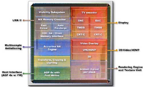
The GeForce4 MX GPU takes up the vast majority (over 70%) of the nForce2 IGP
die area.
Just as was the case with the original nForce, we’d expect system builders and OEMs to capitalize on NVIDIA’s misleading nomenclature by listing their nForce2 products as having GeForce4 graphics. Depending on what speed memory you use with the system, the IGP’s graphics performance will vary somewhere between the speed of a GeForce4 MX 420 and a MX 440.
Just like the original IGP, the nForce2 IGP supports a dual-channel DDR memory architecture that NVIDIA likes to call DualDDR (aka TwinBank). This 128-bit DDR memory bus gives the nForce2 the opportunity to exceed Intel’s 850E chipset in terms of raw memory bandwidth, but as we’ve seen before that only really matters when integrated graphics is enabled. With integrated graphics disabled, the second DDR channel is pretty much useless from a performance standpoint for the vast majority of scenarios.
The nForce2 IGP supports an external AGP 8X interface which will provide users an upgrade path should they decide that they want faster video. The support for AGP 8X comes with perfect timing as NVIDIA will be announcing AGP 8X versions of their GeForce4 line this fall; not to mention that NV30 will be an AGP 8X part as well. Although we don’t expect to see any performance gains from AGP 8X, NVIDIA insists that decoding multiple HDTV streams will quickly saturate AGP 8X; this claim could hint at a future direction for NVIDIA’s Personal Cinema.

Along with the nForce2 IGP, NVIDIA is also introducing the nForce2 System Platform Processor (SPP). The SPP is basically the nForce2 IGP minus the integrated graphics core, meaning that the SPP will be perfect for the majority of the enthusiast market that demands higher performance graphics. All of the features that we’re about to talk about are common to both the nForce2 IGP and SPP.
DualDDR Memory Architecture
The reason that the original nForce was able to offer such compelling integrated graphics performance was because of its dual channel DDR memory controller. Even with DDR400 memory, a 64-bit DDR bus would only be able to offer 3.2GB/s of memory bandwidth, thus going to dual 64-bit memory channels makes a lot of sense.

We’ve proved in the past that the dual channel memory architecture, which NVIDIA is now calling DualDDR, only provides a performance improvement in 3D games with integrated graphics enabled. The reason that adding more memory bandwidth doesn’t improve overall system performance is because the Athlon XP’s FSB is stuck at 133MHz offering up to 2.1GB/s of bandwidth between the Athlon XP and the nForce2 IGP/SPP. With a maximum of 2.1GB/s of data going between the CPU and the IGP/SPP, having twice or even three times that bandwidth between the IGP/SPP and main memory is useless without a memory bandwidth hungry device eating up the remaining bandwidth.
With most I/O taking up less than 100MB/s of bandwidth and audio even less than that, any memory bandwidth offered above and beyond that initial 2.1GB/s goes to waste without integrated graphics enabled. Enabling integrated graphics changes the picture significantly, as we already know that even the 10.4GB/s of bandwidth that the GeForce4 Ti 4600 is allocated isn’t enough at higher resolutions.
The DualDDR setup works identically to TwinBank on the original nForce chipset; with only one DIMM installed, the chipset turns off one of the two 64-bit memory controllers. With a second or third installed, the nForce2 IGP/SPP will enable both memory controllers; and just like the original nForce, you will be able to install DIMMs of different sizes.
If you install two DIMMs, a 128MB and 256MB module then only the first 256MB (smallest memory module size X number of memory modules installed) of memory will be accessible using both 64-bit memory controllers; any memory accessed above 256MB will only be accessed using a single 64-bit channel. The chipset supports up to 3GB of memory and can support 1GB DIMMs in each of its three sockets although stability will be up to the motherboard manufacturers to ensure.
![]() The
DualDDR memory controllers in the nForce2 IGP/SPP support DDR266, 333 and 400
modules. Support for DDR333 and DDR400 really only matters, once again, when
integrated graphics is enabled. NVIDIA’s own internal testing has also
revealed that when the FSB and memory buses are operating synchronously (i.e.
both running at 133MHz DDR), the nForce2 is in its fastest state. This makes
perfect sense seeing as how the additional memory bandwidth is pretty much useless
to the CPU but it isn’t what we’ve seen from VIA for example with
the KT333.
The
DualDDR memory controllers in the nForce2 IGP/SPP support DDR266, 333 and 400
modules. Support for DDR333 and DDR400 really only matters, once again, when
integrated graphics is enabled. NVIDIA’s own internal testing has also
revealed that when the FSB and memory buses are operating synchronously (i.e.
both running at 133MHz DDR), the nForce2 is in its fastest state. This makes
perfect sense seeing as how the additional memory bandwidth is pretty much useless
to the CPU but it isn’t what we’ve seen from VIA for example with
the KT333.
VIA’s KT333 chipset is faster with DDR333 SDRAM than it is with DDR266, although according to NVIDIA the nForce2 running at 266/266 (133MHz DDR FSB and memory bus) is faster than the KT333 running at 266/333 or 266/266. NVIDIA’s approach to this involves using DDR333 but running it synchronously with the FSB and taking advantage of the faster memory by using more aggressive memory timings. We’ve hypothesized that the reason the KT333 runs faster with DDR333 SDRAM is because VIA tuned their memory controller for DDR333 operation while not bothering with optimizing DDR266 performance; given that VIA expects DDR333 to become the memory of choice by the end of this year, this isn’t too far fetched.
To sum things up, if you’re not running with integrated graphics enabled then using DDR333 memory but running it at DDR266 speeds with tighter timings will yield the highest performance on nForce2 according to NVIDIA. With integrated graphics enabled, the highest bandwidth configuration (see table above) will yield the highest performance in 3D applications.
Despite NVIDIA’s assertion that synchronous bus clocking offers the absolute highest performance levels, NVIDIA let us know that end users will be able to asynchronously select FSB, memory and AGP operating frequencies. While this is obviously up to motherboard manufacturer implementations, the potential for independent 1MHz clock increments for each of the aforementioned buses is possible. The biggest benefit this offers is the ability to run the AGP clock within specification while overclocking both the FSB and memory bus.
Dynamic Adaptive Speculative Pre-Processor – Take 2
The nForce2 IGP/SPP also has what NVIDIA is calling a “2nd generation” Dynamic Adaptive Speculative Pre-Processor (DASP). There’s not much information on NVIDIA’s 2nd generation DASP so we’re not able to quantify the improvements NVIDIA made over the original nForce.
As you will remember from our nForce Computer 2001 Preview, NVIDIA’s DASP acts much like the hardware prefetch logic found on Pentium 4s and Athlon XP processors. The logic makes educated guesses about future memory accesses based on where in main memory data was recently accessed from as well as how frequently it was accessed in the past. After making these guesses the logic pre-fetches the data it thinks will be requested into its buffer; should the data be required by the CPU then access latency is reduced by tens of nanoseconds by not requiring a memory access. If the data is never requested by the CPU then it will eventually get replaced in the DASP buffer by other pre-fetched data without incurring a performance hit or gain.
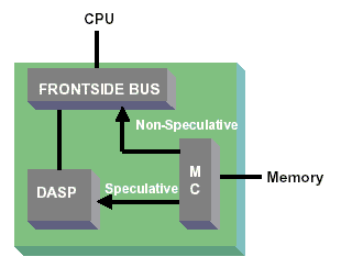
With the original nForce, NVIDIA’s DASP increased performance in synthetic benchmarks by up to 30% and applications such as Adobe Premier and Windows Media Encoder saw a 5 – 10% boost. However, the inclusion of NVIDIA’s DASP logic was not enough to give the nForce chipset a significant performance advantage over the competition. The tuned memory controllers and pre-existing buffers in VIA’s KT266A chipset proved to be more than enough to remain competitive with nForce, and the KT333 even outperformed it. We remain skeptical as to how much of a performance boost this second generation DASP offers but it’s worth mentioning that it is still in there.
Two new MCPs
Although the new IGP and support for new memory speeds are both compelling features of nForce2, NVIDIA’s emphasis remains strong on their Media & Communications Processors (MCP). The MCP acronym, as you’ll remember from the original nForce, is NVIDIA’s version of the classic South Bridge. The MCP is connected to the IGP/SPP via a Hyper Transport link, which makes these MCPs that we’re going to talk about perfect candidates for the forthcoming Hammer/K8 version of the nForce2 chipset. For more information on Hyper Transport’s role in nForce2, take a look at our original nForce preview.
The nForce2 chipset debuts with two MCP offerings: MCP and MCP-T. The basic MCP is a bare MCP that is pin-compatible with the original MCP that was introduced with nForce. This MCP supports USB 2.0, ATA/133 and it has NVIDIA’s own Ethernet MAC. The basic MCP does not have NVIDIA’s Audio Processing Unit (APU) and just basic AC’97 audio support without an integrated DSP. This is the cost effective MCP that can be used on entry-level motherboard designs.
The MCP-T is the more interesting of the two as it builds upon the MCP features by adding IEEE-1394a (Firewire) support, NVIDIA’s APU (unchanged from the original nForce) and a second Ethernet MAC. This second MAC is provided by 3Com, and the combination of the two solutions allows the MCP-T to have “router on a chip” functionality. With two integrated Ethernet MACs, all that’s necessary to enable what NVIDIA calls their DualNet architecture are two relatively cheap Ethernet PHYs to bring two 10/100 Ethernet ports to a nForce2 motherboard. The most obvious configuration is where a broadband Internet connection comes into one of the Ethernet ports with the remaining port on your nForce2 system going out to a switch to provide Internet access to all of the PCs on your network. With Intel’s vision of powerful home PCs acting as content servers to the rest of the house, NVIDIA’s “router on a chip” idea seems to be validated.
Since both of these MCPs interface to the IGP/SPP using Hyper Transport, motherboard manufacturers can reduce costs by using the old nForce 420/415/220 IGPs with the newer MCPs. Also keep in mind that the new MCPs don’t introduce a new APU, so audio quality and DSP performance remain unchanged from the original nForce chipset/MCP.
Standardizing with SoundStorm
 Dolby
Digital encoding support was one of the most talked about features of the original
nForce, but interestingly enough there were some motherboard manufacturers that
didn’t even take advantage of the capability of the original MCP. Although
every motherboard featured analog outputs not all of them shipped with digital
outputs for connecting to an external Dolby Digital decoder.
Dolby
Digital encoding support was one of the most talked about features of the original
nForce, but interestingly enough there were some motherboard manufacturers that
didn’t even take advantage of the capability of the original MCP. Although
every motherboard featured analog outputs not all of them shipped with digital
outputs for connecting to an external Dolby Digital decoder.
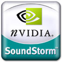
We were first introduced to the nForce’s DD encoding support using NVIDIA’s reference ACR card that enabled 6-channel analog outputs as well as SPDIF audio outputs using optical connectors. NVIDIA took their reference add-in card and branded it as SoundStorm, which is what you see in the picture below.
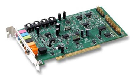
SoundStorm is just another name for NVIDIA’s ACR card that provides all of the inputs and outputs necessary to take advantage of the APU. It is not clear whether or not motherboard manufacturers will be shipping with the rather expensive SoundStorm card, although we’d expect them to continue to use their more cost effective solutions instead.
The Motherboards
NVIDIA has expanded beyond the original 5 launch partners that were chosen for the initial nForce launch to include companies such as Chaintech, EPoX, Leadtek and Soltek for their nForce2 release.


Of course the big names are also ready with their nForce2 solutions, with ABIT, ASUS and MSI coming through once again.

With two different MCPs, the new IGP and the new SPP there are a number of combinations that motherboard manufacturers can exploit using the nForce2 chipset. We’d expect to see cost effective solutions using the nForce2 SPP and the basic MCP and the higher class enthusiast boards offering the new MCP-T. System Integrators and OEMs will demand nForce2 IGP solutions from the motherboard manufacturers and we may even see some configurations using the original nForce IGP in order to cut costs.


As we’ve mentioned before, you won’t be able to pick up any of these boards until the September timeframe; although we will have benchmarks of NVIDIA’s reference board far in advance of that date.
Final Words
NVIDIA has been a PC chipset manufacturer for over a year now, and although they don’t command a large part of the market their nForce platform continues to draw significant amounts of attention. The success of nForce2 will be determined primarily on NVIDIA’s ability to correct the problems the original nForce posed:
• Cost – The first nForce boards were noticeably more expensive than competing solutions from VIA, which was to be expected considering VIA’s very cost oriented manufacturing stance. By the end of the original nForce’s life we saw motherboard prices come down significantly, hopefully some of the combinations of the nForce2 SPP and the new MCP/MCP-T will find their way into cost competitive motherboard solutions.
• Performance – According to NVIDIA, nForce2 is the fastest Socket-A chipset currently available. That is a very bold claim considering that there isn’t a single nForce2 motherboard available to even reviewers for evaluation. NVIDIA is currently in a performance optimization stage with their nForce2 reference boards, and they are quoting performance improvements over KT333 by a few percent at minimum. It would be impressive if NVIDIA can pull it off, but we’re holding all judgments until we see what the third party manufacturers can do come September.
• Time to Market – NVIDIA says it will be September for board availability; if nForce2 is late it definitely won’t bode well for NVIDIA’s chipset track record. While a delayed chipset isn’t nearly as deadly as a missed graphics cycle, enough of these gaps between chipset launches and motherboard releases could be detrimental to NVIDIA’s credibility in the chipset business.
Provided that NVIDIA can address those issues with nForce2 and given that we can trust their performance expectations for the chipset, VIA could finally face some reasonable competition in the Socket-A market. Let’s not forget that NVIDIA’s Hammer solution, codenamed CK8, will be a very close derivative of nForce2 and thus a successful nForce2 launch could translate into promising results with Hammer.
Looking towards the future, NVIDIA does have some very aggressive plans for tomorrow’s nForce chipsets. The highly anticipated successor to the GeForce4 MX, NV31, will find its way into an nForce chipset shortly after its introduction at the beginning of next year. A NV31 equipped nForce chipset could seriously raise the bar of integrated graphics performance beyond what NVIDIA has already been able to do with their latest IGP. While NVIDIA has to play catch-up in garnering market share, it is VIA that will be in a difficult situation if they don’t speed up development of their elusive Columbia GPU.
For now VIA is riding on their experience in developing memory controllers as well as their ability to deliver low-cost solutions to a plethora of customers, but a higher performance integrated graphics core will be necessary moving forward. With Microsoft’s Longhorn OS driven by a 3D GUI, it is very important that the major chipset vendors have powerful integrated graphics cores to suit the needs of the market.
With SiS focusing mainly on the Pentium 4 market and ALi still a no-show, the
final chipset battle in the Socket-A market may come down to VIA vs. NVIDIA.
With VIA already maintaining such a significant lead over NVIDIA, true market
success for the nForce platform may not come along until Hammer makes it big.


