Original Link: https://www.anandtech.com/show/3922/intels-sandy-bridge-architecture-exposed
Intel's Sandy Bridge Architecture Exposed
by Anand Lal Shimpi on September 14, 2010 4:10 AM EST- Posted in
- CPUs
- Intel
- Sandy Bridge
A few weeks ago we previewed the performance of Intel’s next-generation microprocessor architecture, codenamed Sandy Bridge. We came away impressed with our early look at performance but honestly had very little explanation for why the chip performed the way it did. For the first time in years we knew the performance of an Intel processor without knowing much about its underlying architecture.
Today, that all changes.
Sandy Bridge is Intel’s 2011 performance mainstream architecture refresh. It won’t take the place of the 6-core Gulftown based Core i7 processors at the top of the charts, but it’ll occupy the competitive space below it. The value segments won’t see Sandy Bridge until 2012.
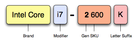
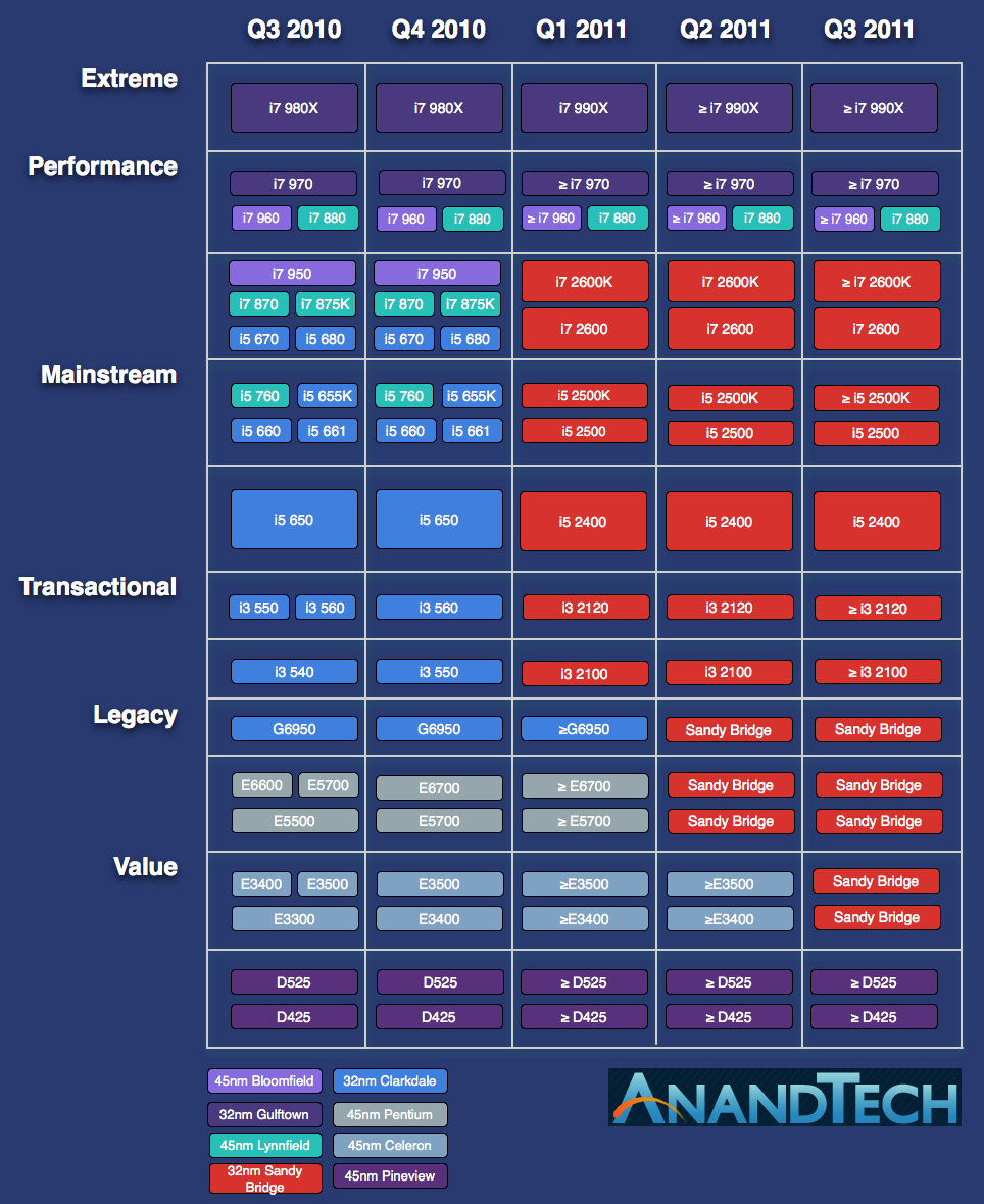
The first CPUs will ship very early in 2011 for both desktops and notebooks. The architecture discussion we have here today applies to both. The CPUs won’t be called Sandy Bridge but instead will be called Intel’s 2nd generation Core i3/i5/i7 microrpocessors. The naming system will follow this format we outlined in our earlier look at Sandy Bridge:
| Sandy Bridge Desktop CPU Comparison | |||||||||
| Base Frequency | L3 Cache | Cores/Threads | Max Single Core Turbo | Intel HD Graphics Frequency/Max Turbo | Unlocked | TDP | |||
| Intel Core i7 2600K | 3.4GHz | 8MB | 4 / 8 | 3.8GHz | 850 / 1350MHz | Y | 95W | ||
| Intel Core i7 2600 | 3.4GHz | 8MB | 4 / 8 | 3.8GHz | 850 / 1350MHz | N | 95W | ||
| Intel Core i5 2500K | 3.3GHz | 6MB | 4 / 4 | 3.7GHz | 850 / 1100MHz | Y | 95W | ||
| Intel Core i5 2500 | 3.3GHz | 6MB | 4 / 4 | 3.7GHz | 850 / 1100MHz | N | 95W | ||
| Intel Core i5 2400 | 3.1GHz | 6MB | 4 / 4 | 3.4GHz | 850 / 1100MHz | N | 95W | ||
| Intel Core i3 2120 | 3.3GHz | 3MB | 2 / 4 | N/A | 850 / 1100MHz | N | 65W | ||
| Intel Core i3 2100 | 3.1GHz | 3MB | 2 / 4 | N/A | 850 / 1100MHz | N | 65W | ||
The CPUs will require a new socket (LGA-1155) and all new motherboards based on Intel’s forthcoming 6-series chipsets.
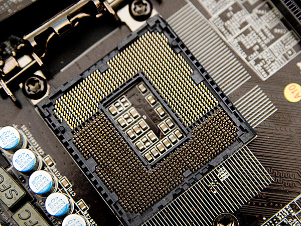
The new socket
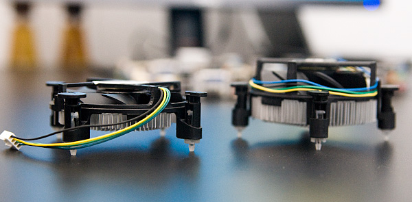
New low-profile 45W Sandy Bridge heatsink (left)
The chipset brings 6Gbps SATA support (2 ports) but no native USB 3, motherboard manufacturers will still have to use an off-chip controller to get USB 3 support. Intel will also enable 5GT/s PCIe 2.0 slots with its 6-series chipsets.
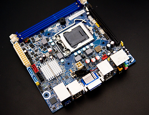
A mini-ITX LGA-1155 Motherboard
The Front End
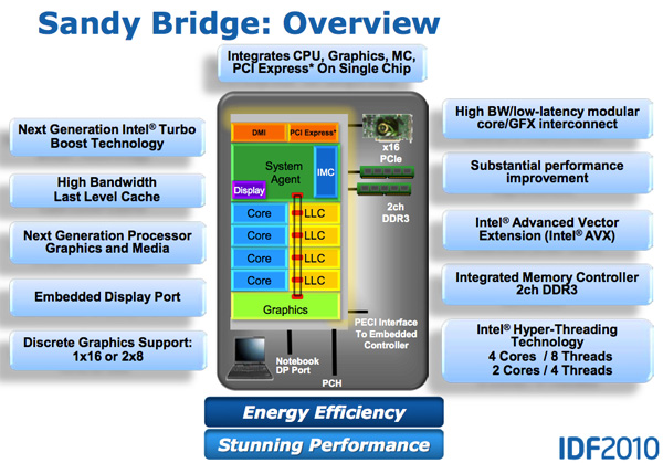
Sandy Bridge’s CPU architecture is evolutionary from a high level viewpoint but far more revolutionary in terms of the number of transistors that have been changed since Nehalem/Westmere.
In Core 2 Intel introduced a block of logic called the Loop Stream Detector (LSD). The LSD would detect when the CPU was executing a software loop turn off the branch predictor and fetch/decode engines and feed the execution units through micro-ops cached by the LSD. This approach saves power by shutting off the front end while the loop executes and improves performance by feeding the execution units out of the LSD.
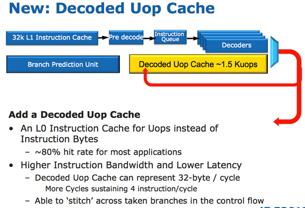
In Sandy Bridge, there’s now a micro-op cache that caches instructions as they’re decoded. There’s no sophisticated algorithm here, the cache simply grabs instructions as they’re decoded. When SB’s fetch hardware grabs a new instruction it first checks to see if the instruction is in the micro-op cache, if it is then the cache services the rest of the pipeline and the front end is powered down. The decode hardware is a very complex part of the x86 pipeline, turning it off saves a significant amount of power. While Sandy Bridge is a high end architecture, I feel that the micro-op cache would probably benefit Intel’s Atom lineup down the road as the burden of x86 decoding is definitely felt in these very low power architectures.
The cache is direct mapped and can store approximately 1.5K micro-ops, which is effectively the equivalent of a 6KB instruction cache. The micro-op cache is fully included in the L1 i-cache and enjoys approximately an 80% hit rate for most applications. You get slightly higher and more consistent bandwidth from the micro-op cache vs. the instruction cache. The actual L1 instruction and data caches haven’t changed, they’re still 32KB each (for total of 64KB L1).
All instructions that are fed out of the decoder can be cached by this engine and as I mentioned before, it’s a blind cache - all instructions are cached. Least recently used data is evicted as it runs out of space.
This may sound a lot like Pentium 4’s trace cache but with one major difference: it doesn’t cache traces. It really looks like an instruction cache that stores micro-ops instead of macro-ops (x86 instructions).
Along with the new micro-op cache, Intel also introduced a completely redesigned branch prediction unit. The new BPU is roughly the same footprint as its predecessor, but is much more accurate. The increase in accuracy is the result of three major innovations.
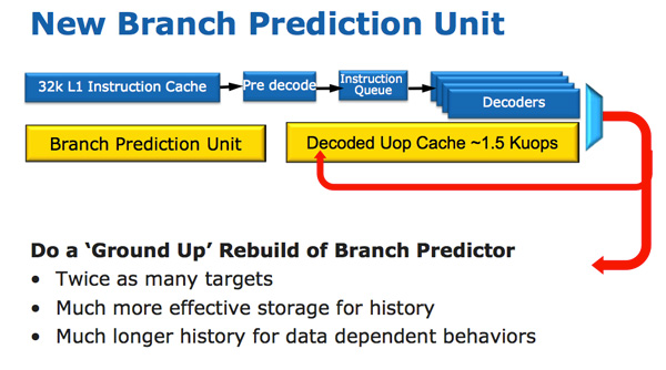
The standard branch predictor is a 2-bit predictor. Each branch is marked in a table as taken/not taken with an associated confidence (strong/weak). Intel found that nearly all of the branches predicted by this bimodal predictor have a strong confidence. In Sandy Bridge, the bimodal branch predictor uses a single confidence bit for multiple branches rather than using one confidence bit per branch. As a result, you have the same number of bits in your branch history table representing many more branches, which can lead to more accurate predictions in the future.
Branch targets also got an efficiency makeover. In previous architectures there was a single size for branch targets, however it turns out that most targets are relatively close. Rather than storing all branch targets in large structures capable of addressing far away targets, SNB now includes support for multiple branch target sizes. With smaller target sizes there’s less wasted space and now the CPU can keep track of more targets, improving prediction speed.
Finally we have the conventional method of increasing the accuracy of a branch predictor: using more history bits. Unfortunately this only works well for certain types of branches that require looking at long patterns of instructions, and not well for shorter more common branches (e.g. loops, if/else). Sandy Bridge’s BPU partitions branches into those that need a short vs. long history for accurate prediction.
A Physical Register File
Just like AMD announced in its Bobcat and Bulldozer architectures, in Sandy Bridge Intel moves to a physical register file. In Core 2 and Nehalem, every micro-op had a copy of every operand that it needed. This meant the out-of-order execution hardware (scheduler/reorder buffer/associated queues) had to be much larger as it needed to accommodate the micro-ops as well as their associated data. Back in the Core Duo days that was 80-bits of data. When Intel implemented SSE, the burden grew to 128-bits. With AVX however we now have potentially 256-bit operands associated with each instruction, and the amount that the scheduling/reordering hardware would have to grow to support the AVX execution hardware Intel wanted to enable was too much.
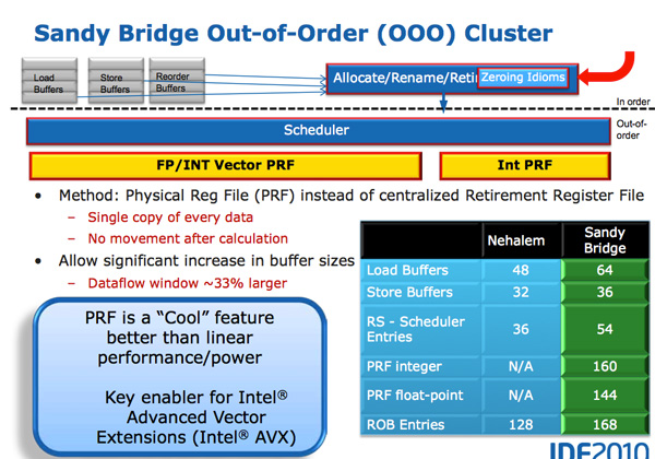
A physical register file stores micro-op operands in the register file; as the micro-op travels down the OoO engine it only carries pointers to its operands and not the data itself. This significantly reduces the power of the out of order execution hardware (moving large amounts of data around a chip eats tons of power), it also reduces die area further down the pipe. The die savings are translated into a larger out of order window.
The die area savings are key as they enable one of Sandy Bridge’s major innovations: AVX performance.
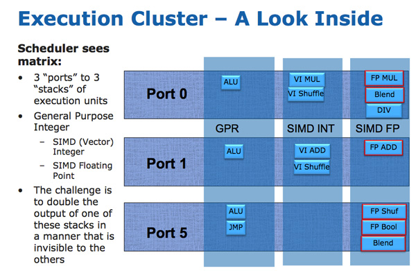
The AVX instructions support 256-bit operands, which as you can guess can eat up quite a bit of die area. The move to a physical register file enabled Intel to increase OoO buffers to properly feed a higher throughput floating point engine. Intel clearly believes in AVX as it extended all of its SIMD units to 256-bit wide. The extension is done at minimal die expense. Nehalem has three execution ports and three stacks of execution units:
Sandy Bridge allows 256-bit AVX instructions to borrow 128-bits of the integer SIMD datapath. This minimizes the impact of AVX on the execution die area while enabling twice the FP throughput, you get two 256-bit AVX operations per clock (+ one 256-bit AVX load).
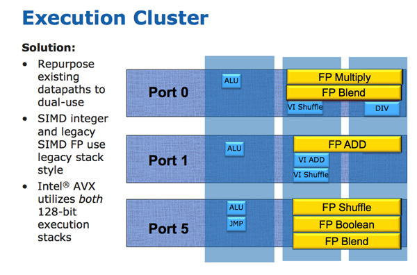
Granted you can’t mix 256-bit AVX and 128-bit integer SSE ops, however remember SNB now has larger buffers to help extract more ILP.
The upper 128-bits of the execution hardware and paths are power gated. Standard 128-bit SSE operations will not incur an additional power penalty as a result of Intel’s 256-bit expansion.
AMD sees AVX support in a different light than Intel. Bulldozer features two 128-bit SSE paths that can be combined for 256-bit AVX operations. Compared to an 8-core Bulldozer a 4-core Sandy Bridge has twice the 256-bit AVX throughput. Whether or not this is an issue going forward really depends on how well AVX is used in applications.
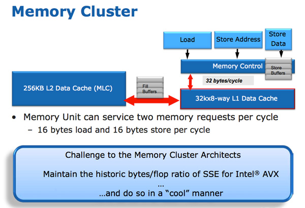
The improvements to Sandy Bridge’s FP performance increase the demands on the load/store units. In Nehalem/Westmere you had three LS ports: load, store address and store data.
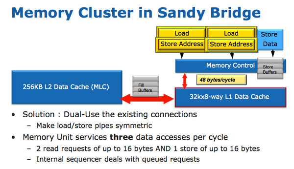
In SNB, the load and store address ports are now symmetric so each port can service a load or store address. This doubles the load bandwidth which is important as Intel doubled the peak floating point performance in Sandy Bridge.
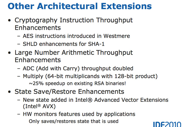
There are some integer execution improvements in Sandy Bridge, although they are more limited. Add with carry (ADC) instruction throughput is doubled, while large scale multiplies (64 * 64) see a ~25% speedup.
The Ring Bus
With Nehalem/Westmere all cores, whether dual, quad or six of them, had their own private path to the last level (L3) cache. That’s roughly 1000 wires per core. The problem with this approach is that it doesn’t work well as you scale up in things that need access to the L3 cache.
Sandy Bridge adds a GPU and video transcoding engine on-die that share the L3 cache. Rather than laying out another 2000 wires to the L3 cache Intel introduced a ring bus.
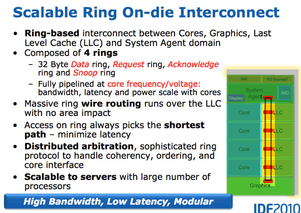
Architecturally, this is the same ring bus used in Nehalem EX and Westmere EX. Each core, each slice of L3 (LLC) cache, the on-die GPU, media engine and the system agent (fancy word for North Bridge) all have a stop on the ring bus.
The bus is made up of four independent rings: a data ring, request ring, acknowledge ring and snoop ring. Each stop for each ring can accept 32-bytes of data per clock. As you increase core count and cache size, your cache bandwidth increases accordingly.
Per core you get the same amount of L3 cache bandwidth as in high end Westmere parts - 96GB/s. Aggregate bandwidth is 4x that in a quad-core system since you get a ring stop per core (384GB/s).
L3 latency is significantly reduced from around 36 cycles in Westmere to 26 - 31 cycles in Sandy Bridge. We saw this in our Sandy Bridge preview and now have absolute numbers in hand. The variable cache latency has to do with what core is accessing what slice of cache.
Also unlike Westmere, the L3 cache now runs at the core clock speed - the concept of the un-core still exists but Intel calls it the “system agent” instead and it no longer includes the L3 cache.
With the L3 cache running at the core clock you get the benefit of a much faster cache. The downside is the L3 underclocks itself in tandem with the processor cores. If the GPU needs the L3 while the CPUs are downclocked, the L3 cache won’t be running as fast as it could had it been independent.
The L3 cache is divided into slices, one associated with each core although each core can address the entire cache. Each slice gets its own stop and each slice has a full cache pipeline. In Westmere there was a single cache pipeline and queue that all cores forwarded requests to, in Sandy Bridge it’s distributed per cache slice.
The ring wire routing runs entirely over the L3 cache with no die area impact. This is particularly important as you effectively get more cache bandwidth without any increase in die area. It also allows Intel to scale the core count and cache size without incurring additional ring-related die area.
Each of the consumers/producers on the ring get their own stop. The ring always takes the shortest path. Bus arbitration is distributed on the ring, each stop knows if there’s an empty slot on the ring one clock before.
The System Agent
For some reason Intel stopped using the term un-core, instead in Sandy Bridge it’s called the System Agent.
The System Agent houses the traditional North Bridge. You get a 16 PCIe 2.0 lanes that can be split into two x8s. There’s a redesigned dual-channel DDR3 memory controller that finally restores memory latency to around Lynnfield levels (Clarkdale moved the memory controller off the CPU die and onto the GPU).
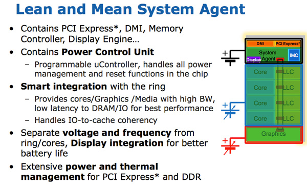
The SA also has the DMI interface, display engine and the PCU (Power Control Unit). The SA clock speed is lower than the rest of the core and it is on its own power plane.
Sandy Bridge Graphics
The largest performance improvement on Sandy Bridge vs. current Westmere architectures actually has nothing to do with the CPU, it’s all graphics. While the CPU cores show a 10 - 30% improvement in performance, Sandy Bridge graphics performance is easily double what Intel delivered with Clarkdale/Arrandale at the beginning of the year.
While the ‘dales improved performance by moving graphics to a 45nm process, increasing shader hardware and clock speed, SNB graphics improves through a significant increase in IPC.
The Sandy Bridge GPU is on-die built out of the same 32nm transistors as the CPU cores. The GPU is on its own power island and clock domain. The GPU can be powered down or clocked up independently of the CPU. Graphics turbo is available on both desktop and mobile parts, and you get more bins with graphics turbo on Sandy Bridge than you did with Arrandale.
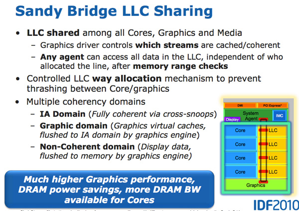
The GPU is treated like an equal citizen in the Sandy Bridge world, it gets equal access to the L3 cache. The graphics driver controls what gets into the L3 cache and you can even limit how much cache the GPU is able to use. Storing graphics data in the cache is particularly important as it saves trips to main memory which are costly from both a performance and power standpoint. Redesigning a GPU to make use of a cache isn’t a simple task. It usually requires the sort of complete re-design that NVIDIA did with GF100 for example.
SNB graphics is the anti-Larrabee. While Larrabee focused on extensive use of fully programmable hardware (with the exception of the texture hardware), SNB graphics (internally referred to as Gen 6 graphics) makes extensive use of fixed function hardware. The design mentality was anything that could be described by a fixed function should be implemented in fixed function hardware. The benefit is performance/power/die area efficiency, at the expense of flexibility. Keeping much of the GPU fixed function is in-line with Intel’s CPU centric view of the world. By contrast, taking the GPU as programmable as possible makes more sense for a GPU focused company like NVIDIA.
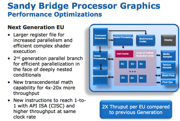
The programmable shader hardware is composed of shaders/cores/execution units that Intel calls EUs. Each EU can dual issue picking instructions from multiple threads. The internal ISA maps one-to-one with most DirectX 10 API instructions resulting in a very CISC-like architecture. Moving to one-to-one API to instruction mapping increases IPC by effectively increasing the width of the EUs.
There are other improvements within the EU. Transcendental math is handled by hardware in the EU and its performance has been sped up considerably. Intel told us that sine and cosine operations are several orders of magnitude faster now than they were in current HD Graphics.
In previous Intel graphics architectures the register file was repartitioned on the fly. If a thread needed fewer registers, the remaining registers could be allocated to another thread. While this was a great approach for saving die area, it proved to be a limiter for performance. In many cases threads couldn’t be worked on as there were no registers available for use. Prior to Intel HD Graphics each thread had an average of 64 registers, the ‘dales brought that average up to 80 per thread. In SNB, the GPU has a fixed amount of registers per thread: 120. The register count limiting thread count scenarios have been alleviated.
All of these enhancements result in 2x the instruction throughput per EU compared to Intel’s HD Graphics today.

Sandy Bridge vs. NVIDIA GeForce 310M Playing Starcraft 2
At launch there will be two versions of Sandy Bridge graphics: one with 6 EUs and one with 12 EUs. All mobile parts (at launch) will use 12 EUs, while desktop SKUs may either use 6 or 12 depending on the model. From what I’ve heard, the higher end SKUs may have 12 while the lower end models will have 6 but I haven’t seen it on a roadmap yet so I can’t confirm. With a 2x improvement in throughput per EU, you should see greater than Intel HD Graphics performance even with the 6 EU parts (thanks to higher clock speeds and the GPU sharing the L3 cache).
Sandy Bridge Media Engine
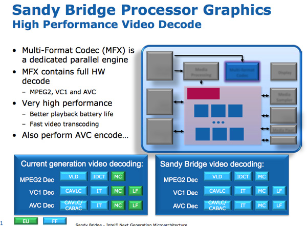
Sitting alongside the GPU is Sandy Bridge’s Media processor. Media processing in SNB is composed of two major components: video decode, and video encode.
The hardware accelerated decode engine is improved from the current generation: the entire video pipeline is now decoded via fixed function units. This is contrast to Intel’s current design that uses the EU array for some video decode stages. As a result, Intel claims that SNB processor power is cut in half for HD video playback.
The video encode engine is a brand new addition to Sandy Bridge. Intel is being light on the details of the encoder but we saw a demo where Intel took a ~3 minute 1080p 30Mbps source video and transcoded it to a 640 x 360 iPhone video format. The total process took 14 seconds and completed at a rate of roughly 400 frames per second.
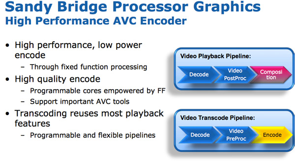
Given Intel’s close relationship with many software vendors who work on video transcoding, I wouldn’t be surprised if we saw decent support for SNB’s video encoding engine at launch. At 400 fps we’re well in the realm of high end GPU encoding performance, despite being run on a 3mm^2 piece of the Sandy Bridge die.
New, More Aggressive Turbo
Lynnfield was the first Intel CPU to aggressively pursue the idea of dynamically increasing the core clock of active CPU cores while powering down idle cores. The idea is that if you have a 95W TDP for a quad-core CPU, but three of those four cores are idle, then you can increase the clock speed of the one active core until you hit that TDP limit.
In all current generation processors the assumption is that the CPU reaches that TDP immediately upon enabling turbo. In reality however, the CPU doesn’t heat up immediately - there’s a period of time where the CPU isn’t dissipating its full TDP - there’s a ramp.
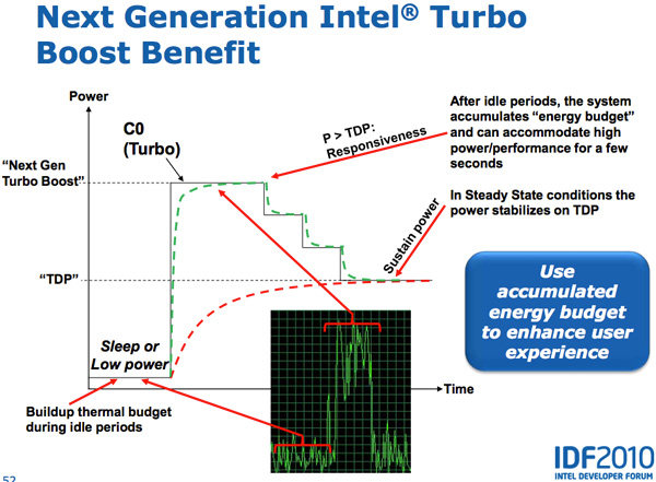
Sandy Bridge takes advantage of this by allowing the PCU to turbo up active cores above TDP for short periods of time (up to 25 seconds). The PCU keeps track of available thermal budget while idle and spends it when CPU demand goes up. The longer the CPU remains idle, the more potential it has to ramp up above TDP later on. When a workload comes around, the CPU can turbo above its TDP and step down as the processor heats up, eventually settling down at its TDP.
While SNB can turbo up beyond its TDP, the PCU won’t allow the chip to exceed any reliability limits (similar to turbo today).
In addition to above-TDP-turbo, Sandy Bridge will also support more turbo bins than Nehalem/Westmere. Intel isn’t disclosing how much more turbo headroom we’ll have, but the additional bins are at least visible with multiple cores active. Current designs usually only turbo up one or two bins with all four cores active, I’d expect to see another bin or two there and possibly more in lighter load cases.
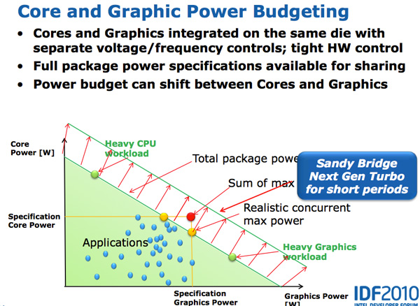
Both CPU and GPU turbo can work in tandem. Workloads that are more GPU bound running on SNB can result in the CPU cores clocking down and the GPU clocking up, while CPU bound tasks can drop the GPU frequency and increase CPU frequency.
Sandy Bridge as a whole is much more dynamic of a beast than anything that’s come before it.
Multiplier-only Overclocking
There's no new information on Sandy Bridge overclocking at this point (although it's looking increasingly likely that there will be a reasonably priced K-series SKU for those users who want the flexibility to overclock without spending $1000). I've included the overclocking text and roadmap from our Sandy Bridge Preview below if you're interested in seeing what Intel has planned.
It wasn’t until the Pentium II that Intel started shipping multiplier locked CPUs. Before then you could set the multiplier on your CPU to anything that was supported by the line, and if you had a good chip and good enough cooling you just overclocked your processor. Intel’s policies changed once remarking, the process of relabeling and reselling a lower spec CPU as a higher one, started to take off.
While multipliers were locked, Intel left FSB overclocking open. That would be an end user or system integrator decision and not something that could be done when selling an individual CPU. However, ever since before the Pentium III Intel had aspirations of shipping fully locked CPUs. The power of the enthusiast community generally kept Intel from exploring such avenues, but we live in different times today.
Two things have changed Intel’s feelings on the topic. First and foremost is the advent of Turbo Boost. So long as Intel doesn’t artificially limit turbo modes, we now have the ability to run CPUs at whatever clock speed they can run at without exceeding thermal or current limits. We saw the first really exciting Turbo with Lynnfield, and Sandy Bridge is going to expand on that as well. On the flip side, Intel has used Turbo as a marketing differentiator between parts so there’s still a need to overclock.
The second major change within Intel is the willingness to directly address the enthusiast community with unlocked K-series SKUs. We saw this recently with the Core i7 875K and Core i5 655K parts that ship fully unlocked for the overclocking community.
The K-series SKUs, these will be more important with Sandy Bridge
With Sandy Bridge, Intel integrated the clock generator, usually present on the motherboard, onto the 6-series chipset die. While BCLK is adjustable on current Core iX processors, with Sandy Bridge it’s mostly locked at 100MHz. There will be some wiggle room as far as I can tell, but it’s not going to be much. Overclocking, as we know it, is dead.
Well, not exactly.
Intel makes three concessions.
First and foremost we have the K-series parts. These will be fully unlocked, supporting multipliers up to 57x. Sandy Bridge should have more attractive K SKUs than what we’ve seen to date. The Core i7 2600 and 2500 will both be available as a K-edition. The former should be priced around $562 and the latter at $205 if we go off of current pricing.
Secondly, some regular Sandy Bridge processors will have partially unlocked multipliers. The idea is that you take your highest turbo multiplier, add a few more bins on top of that, and that’ll be your maximum multiplier. It gives some overclocking headroom, but not limitless. Intel is still working out the details for how far you can go with these partially unlocked parts, but I’ve chimed in with my opinion and hopefully we’ll see something reasonable come from the company. I am hopeful that these partially unlocked parts will have enough multipliers available to make for decent overclocks.
Finally, if you focus on multiplier-only overclocking you lose the ability to increase memory bandwidth as you increase CPU clock speed. The faster your CPU, the more data it needs and thus the faster your memory subsystem needs to be in order to scale well. As a result, on P67 motherboards you’ll be able to adjust your memory ratios to support up to DDR3-2133.
Personally, I’d love nothing more than for everything to ship unlocked. The realities of Intel’s business apparently prevent that, so we’re left with something that could either be a non-issue or just horrible.
If the K-series parts are priced appropriately, which at first indication it seems they will be, then this will be a non-issue for a portion of the enthusiast market. You’ll pay the same amount for your Core i7 2500K as you would for a Core i5 750 and you’ll have the same overclocking potential.
Regardless of how they’re priced, what this is sure to hurt is the ability to buy a low end part like the Core i3 530 and overclock the crap out of it. What Intel decides to do with the available multiplier headroom on parts further down the stack is unknown at this point. If Intel wanted to, it could pick exciting parts at lower price points, give them a few more bins of overclocking headroom and compete in a more targeted way with AMD offerings at similar price points. A benevolent Intel would allow enough headroom as the parts can reliably hit with air cooling.
The potential for this to all go very wrong is there. I’m going to reserve final judgment until I get a better idea for what the Sandy Bridge family is going to look like.
Final Words
Intel is trying out a new approach to sharing information about its technologies. In an attempt to surprise the market (and potentially positively impact stock price), Intel is keeping details on upcoming products quiet until it gets closer to launch. This is why we didn’t hear about Sandy Bridge until after we were able to preview its performance a couple of weeks ago. I can’t say I’m a fan of the new approach, but it does make things a little more exciting.
And exciting Sandy Bridge is. The CPU architecture itself doesn’t look too revolutionary. These are the sorts of improvements we’ve come to expect from Intel from one generation to the next. The out of order execution window grew as did all associated buffers. Thanks to some significant redesigns in hardware Intel was able to increase branch prediction accuracy and FP execution throughput all while making the chip more energy efficient.
Improved turbo will surely be appreciated. More aggressive turbo bins plus the ability to turbo up above TDP limits for short periods of time will help make PCs feel more responsive even when doing relatively benign tasks. Things like launching applications, loading web pages or just opening new window stand to benefit.
The architecture sounds a lot like Intel simply did Nehalem/Westmere better. Over time you come up with newer, better ways to do things and that’s ultimately what Sandy Bridge looks like - a better, more efficient way to do what Conroe, Nehalem and Westmere did before it.
The more dramatic changes happened outside of the cores. GPU performance is clearly an important Sandy Bridge feature as we’ve already shown. I can’t help but be curious about how far Intel could take its SNB graphics subsystem if it simply scaled up the number of EUs. The media processing engine, particularly with the video transcode support is very exciting. Assuming image quality is maintained and there’s good software support at launch, this could very well be Sandy Bridge’s killer feature. The ability to transcode at over 10x real time on everything from a desktop to a notebook is just awesome. With good software support, SNB’s video transcode engine could effectively stop consumer GPU based video encoding in its tracks. The improved video decode engine is also a welcome addition to the Sandy Bridge architecture.
Connecting it all together we have Sandy Bridge’s ring bus. Generally microprocessor designs don’t undergo such a radical changes unless the design will be used for a while to come. The ring bus sounds very scalable and should support growth in core count, L3 cache and GPU performance. This may end up being the base architecture that takes us from multi-core to many core.
Mobile Sandy Bridge is significantly faster than Arrandale/Clarksfield
Sandy Bridge will ship in Q1 2011 for both notebooks and desktops and from what we’ve heard, pricing will be very compelling. If you're interested in a sneak peak of Sandy Bridge's performance, take a look at our preview here.


