Original Link: https://www.anandtech.com/show/4098/nvidias-tegra-2-take-two-more-architectural-details-and-design-wins
NVIDIA's Tegra 2 Take Two: More Architectural Details and Design Wins
by Anand Lal Shimpi on January 5, 2011 2:51 PM EST- Posted in
- Motorola Droid
- Tegra 2
- LG
- Smartphones
- Optimus 2X
- ATRIX 4G
- Mobile
- NVIDIA
Twelve months ago NVIDIA stood on stage at CES and introduced its Tegra 2 SoC. It promised dozens of design wins and smartphones shipping before Spring 2010. That obviously did not happen.
What instead happened was NVIDIA lost a number of design wins, many of which we centered around mobile OSes other than Android. There were a number of Windows Mobile/Windows CE based designs that never made it to market, and a lot of efforts around earlier versions of Android that never went anywhere.
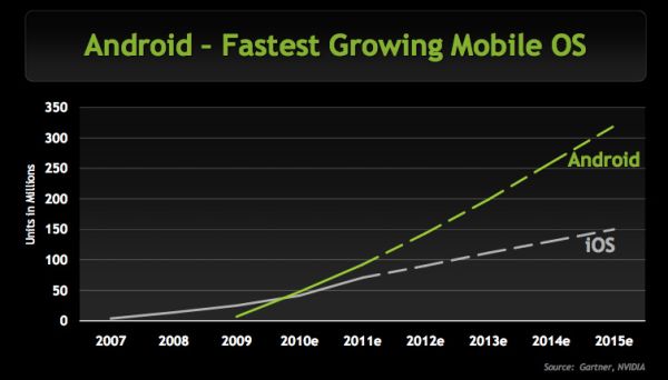
In the time since NVIDIA’s CES 2010 announcement, the company has shifted resources and focused its entire Tegra team on a single OS: Android. Choosing Android isn’t a hard decision to understand, of all of the available smartphone OS options it has the most momentum behind it.
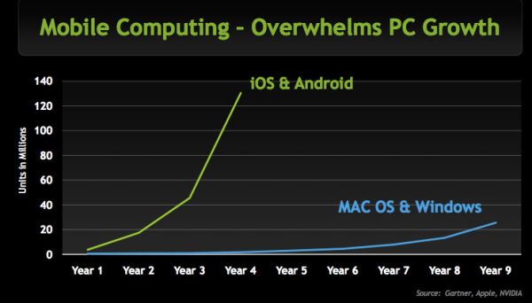
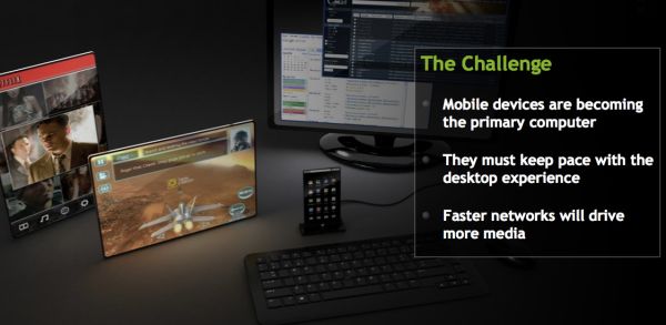
NVIDIA views the smartphone space like a condensed evolution of what happened in the PC industry. In fact, NVIDIA believes that within the next decade, mainstream PCs will actually be smartphones. You’ll simply connect your smartphone to a wireless display and keyboard/mouse when you’re at your desk, and just take it with you when you’re on the move. This usage model won’t replace high end PCs, but for anything you’d find in the mainstream market it should be sufficient.
Motorola’s recently announced ATRIX 4G and webtop dock is the perfect example of this type of a usage model, although it is a very early precursor to what NVIDIA believes is the future of mainstream computing.
NVIDIA thus expects the smartphone market to evolve very similarly to how the desktop PC market evolved - including being driven by gaming. The Tegra 2 SoC is NVIDIA’s first honest attempt at addressing this market and with today’s announcements from LG and Motorola, NVIDIA is actually gaining some traction.
The CPU: A Dual-Core ARM Cortex A9
NVIDIA is a traditional ARM core licensee, which means it implements ARM’s own design rather than taking the instruction set and designing its own core around it (ala Qualcomm).
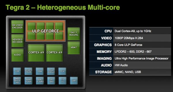
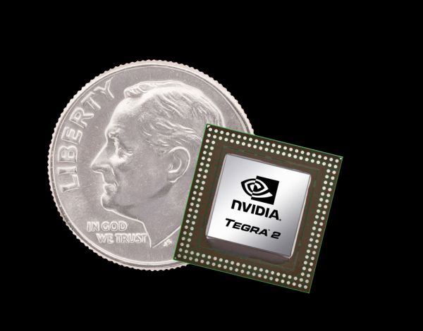
The Tegra 2 SoC has a pair of ARM Cortex A9s running at up to 1GHz. The cores are clock gated but not power gated. Clock speed is dynamic and can be adjusted at a very granular level depending on load. Both cores operate on the same power plane.
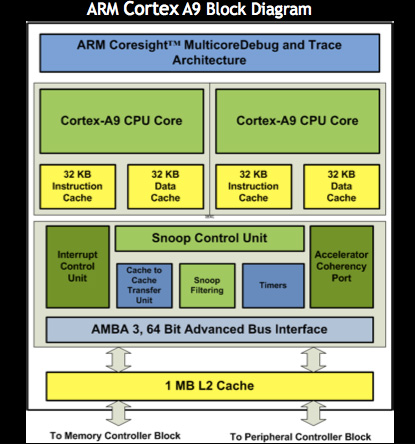
Architecturally, the Cortex A9 isn’t very different from the Cortex A8. The main change is a move from a dual-issue in order architecture with the A8 to a dual-issue out-of-order architecture with the A9.
With its OoO architecture, the A9 adds a re-order buffer and 16 more general purpose registers over the A8 for register renaming. Cortex A9 can reorder around write after read and write after write hazards.
ARM’s Cortex A9 MPcore architecture supports up to four cores behind a single shared L2 cache (at up to 1MB in size). Tegra 2 implements a full 1MB shared L2 cache and two Cortex A9 cores. Each core has a 64KB L1 cache (32KB instruction + 32KB data cache).
Pipeline depth is another major change between A8 and A9. While the Cortex A8 had a 13-cycle branch mispredict penalty, A9 shortens the pipeline to 8 cycles. The shallower pipeline improves IPC and reduces power consumption. Through process technology hitting 1GHz isn’t a problem at TSMC 40nm.
From what I can tell, branch prediction, TLBs and execution paths haven’t changed between A8 and A9 although I’m still awaiting further details from ARM on this.
NVIDIA is claiming the end result is a 20% increase in IPC between A8 and A9. That’s actually a bit lower than I’d expect, but combined with the move to dual core you should see a significant increase in performance compared to current Snapdragon and A8 based devices.
If on single threaded workloads the best performance improvement we see is 20%, Qualcomm’s dual-core 1.2GHz Snapdragon due out later this year could still be performance competitive.
While all Cortex A8 designs incorporated ARM’s SIMD engine called NEON, A9 gives you the option of integrating either a SIMD engine (ARM’s Media Processing Engine, aka NEON) or a non-vector floating point unit (VFPv3-D16). NVIDIA chose not to include the A9’s MPE and instead opted for the FPU. Unlike the A8’s FPU, in the A9 the FPU is fully pipelined - so performance is much improved. The A9’s FPU however is still not as quick at math as the optional SIMD MPE.
| Minimum Instruction Latencies (Single Precision) | ||||||
| Instruction | FADD | FSUB | FMUL | FMAC | FFDIV | FSQRT |
| ARM Cortex A8 (FPU) | 9 cycles | 9 cycles | 10 cycles | 18 cycles | 20 cycles | 19 cycles |
| ARM Cortex A9 (FPU) | 4 cycles | 4 cycles | 5 cycles | 8 cycles | 15 cycles | 17 cycles |
| ARM Cortex A8 (NEON) | 1 cycle | 1 cycle | 1 cycle | 1 cycle | N/A | N/A |
| ARM Cortex A9 (MPE/NEON) | 1 cycle | 1 cycle | 1 cycle | 1 cycle | 10 cycles | 13 cycles |
NVIDIA claims implementing MPE would incur a 30% die penalty for a performance improvement that impacts only a minimal amount of code. It admits that at some point integrating a SIMD engine makes sense, just not yet. The table above shows a comparison of instruction latency on various floating point and SIMD engines in A8 and A9.
TI’s OMAP 4 on the other hand will integrate ARM’s Cortex A9 MPE. Depending on the code being run, OMAP 4 could have a significant performance advantage in some cases.
The GeForce ULV GPU
Tegra 2 integrates the GeForce ULV, an NVIDIA designed OpenGL ES 2.0 GPU.
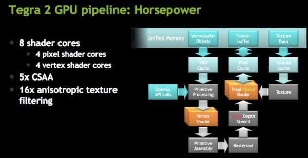
At a high level NVIDIA is calling the GeForce ULV an 8-core GPU, however its not a unified shader GPU. Each core is an ALU but half of them are used for vertex shaders and the other half are for pixel shaders. You can expect the GeForce ULV line to take a similar evolutionary path to desktop GeForce in the future.
The four vertex shader cores/ALUs can do a total of 4 MADDs per clock, the same is true for the four pixel shader ALUs (4 MADDs per clock).
For those of you who follow NVIDIA’s desktop architecture: at the front end the machine works on a 4-thread warp, where each thread is a single pixel.
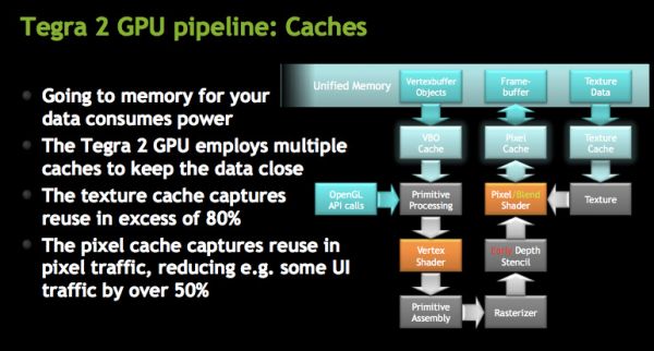
Architecturally, the GeForce ULV borrows several technologies that only recently debuted on desktop GPUs. GeForce ULV has a pixel cache, a feature that wasn’t introduced in GeForce on the desktop until Fermi. This is purely an efficiency play as saving any trips to main memory reduces power consumption considerably (firing up external interfaces always burns watts quicker than having data on die).
NVIDIA also moved the register files closer to the math units, again in the pursuit of low power consumption. GeForce ULV is also extremely clock gated although it’s not something we’re able to quantify.
NVIDIA did reduce the number of pipeline stages compared to its desktop GPUs by a factor of 2.5 to keep power consumption down.
The GeForce ULV supports Early Z culling, a feature first introduced on the desktop with G80. While G80 could throw away around 64 pixels per clock, early Z on GeForce ULV can throw away 4 pixels per clock.
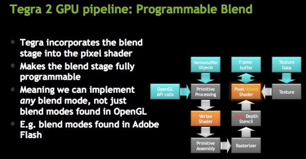
The ROPs are integrated into the pixel shader, making what NVIDIA calls a programmable blend unit. GeForce ULV uses the same ALUs for ROPs as it does for pixel shaders. This hardware reuse saves die size although it adds control complexity to the design. The hardware can perform one texture fetch and one ROP operation per clock.
While GeForce ULV supports texture compression, it doesn’t support frame buffer compression.
Both AA and AF are supported by GeForce ULV. NVIDIA supports 5X coverage sample AA (same CSAA as we have on the desktop) and up to 16X anisotropic filtering.
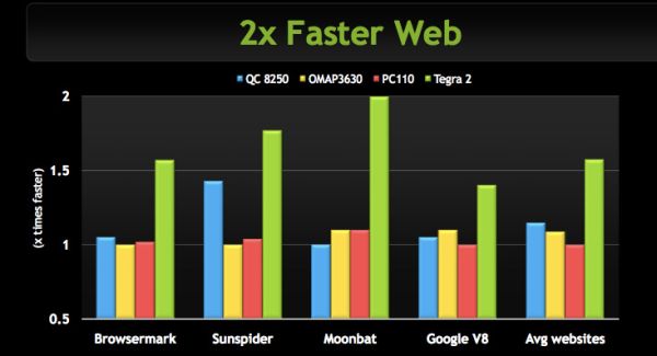
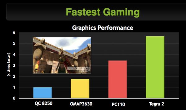
We’ve done a little bit of performance testing of Tegra 2’s GPU vs. the PowerVR SGX 530/540 and Qualcomm’s Adreno 200/205. It’s too soon for us to publish Tegra 2 smartphone performance numbers, but the numbers NVIDIA is sharing with us show a huge advantage over competitive GPUs. In our own experience we’ve found that Tegra 2’s GPU is a bit faster than the PowerVR SGX 540, but nothing lines up with the numbers NVIDIA has shown us thus far. We’re still a couple of months away from final software and driver builds so it’s possible that things will change.
Memory Controller
NVIDIA’s Tegra 2 only has a single 32-bit LPDDR2 memory controller, but supports running it at up to 600MHz (667MHz with standard DDR2). By comparison, TI is using two 32-bit LPDDR2 memory channels on its OMAP 4. NVIDIA claims that its expertise in designing GPU memory controllers allowed it to get by with only a single 32-bit LPDDR2 memory controller. NVIDIA stayed away from going with a dual-channel interface in order to keep power consumption down.
Video Decode Engine
NVIDIA claims the Tegra 2’s video decoder can decode 1080p H.264 baseline profile (no CABAC) at 20Mbps while only drawing 400mW. The power draw numbers seem suspiciously low but we’ll have to test that for ourselves once we can get our hands on Tegra 2 smartphones in the coming months.
Full Flash GPU Acceleration
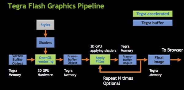
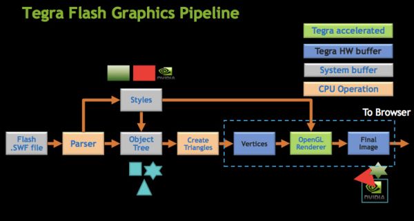
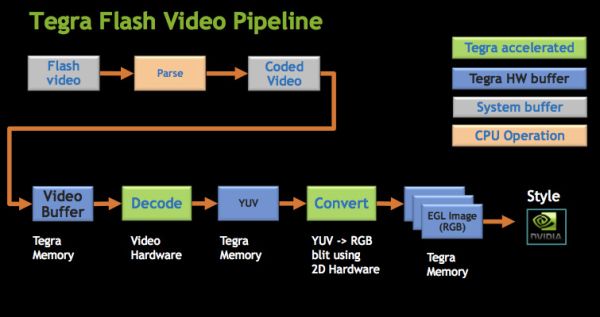
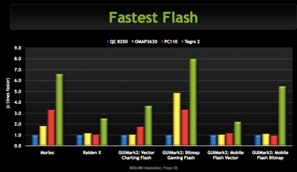
Borrowing another aspect from the desktop GPU segment, Tegra 2 can fully accelerate flash video and flash content in hardware.
Integrated Image Signal Processor
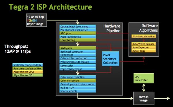
NVIDIA is also releasing a little more information about its custom ISP (Image Signal Processor) inside Tegra 2.
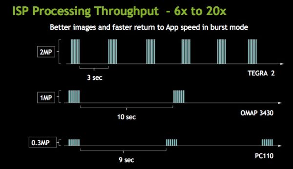
While it’s too early to tell anything about the quality of Tegra 2 smartphone cameras, NVIDIA’s ISP is extremely high performance. The ISP can burst through 12MP images at 11 frames per second.
LG’s Optimus 2X uses the Tegra 2’s fast ISP to be able to shoot in a burst mode that fires off 6 shots in sequence without interruption.
Tegra Optimized Smartphone Games: Tegra Zone
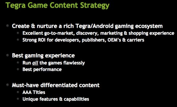
For NVIDIA to build a name for itself in the smartphone and tablet space, its SoCs have to offer something different. Being the first to dual core is a nice thing to brag about but Qualcomm and TI will be shipping dual core SoCs in 2011 as well. NVIDIA views its close relationship with console and PC game developers as one of its major strengths in the market. NVIDIA hopes to leverage its developer relations as a Tegra platform advantage.
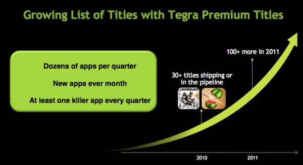
The how is really quite simple. NVIDIA is working with many of its existing partners as well as some new ones in the smartphone space to release Tegra optimized titles for Android every quarter. The goal is to have at least one killer title every quarter. By the end of 2011 NVIDIA expects to have over 100 Tegra optimized titles available.
The titles will be available through a custom marketplace on Android called Tegra Zone. All Tegra 2 enabled phones will have the Tegra Zone app that you can use to find, purchase and download Tegra optimized games.
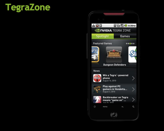
The purchase process works over the Android Market system, you just purchase from within the Tegra Zone app instead of using Market.
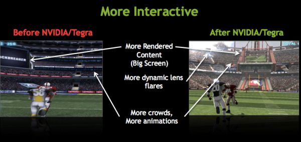
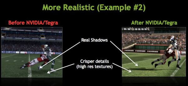
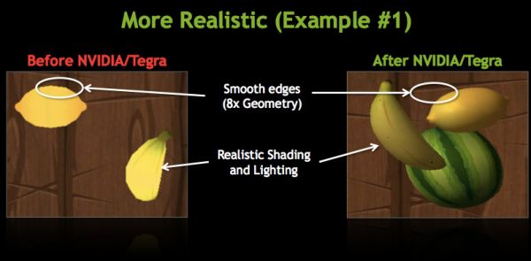
NVIDIA provided a few examples of what Tegra 2 optimized games could look like. Below is a quick comparison between Backbreaker running on iOS and Tegra 2:
Turn up detail and quality settings, include some more visuals and you’ve got the gist of the difference between a Tegra 2 game and a regular title.
The difference is nice but I personally don’t feel like it’s enough by itself to move users to Tegra 2 based phones. It’s simply a nice adder for Tegra 2 owners. Ultimately it’s performance, battery life and the quality of the devices that will sell NVIDIA based handsets.
Working with developers this early on gives you a hint at NVIDIA’s future smartphone strategy. NVIDIA sees gaming as a huge part of what will drive smartphone innovation in the future, so if you look back at NVIDIA’s strategy from the early days of 3D gaming on the PC you can probably get a good idea of what to expect from Tegra in the future.
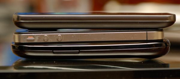
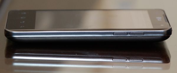
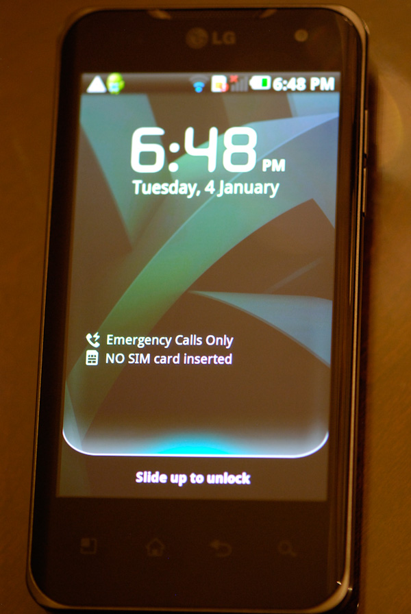
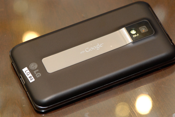
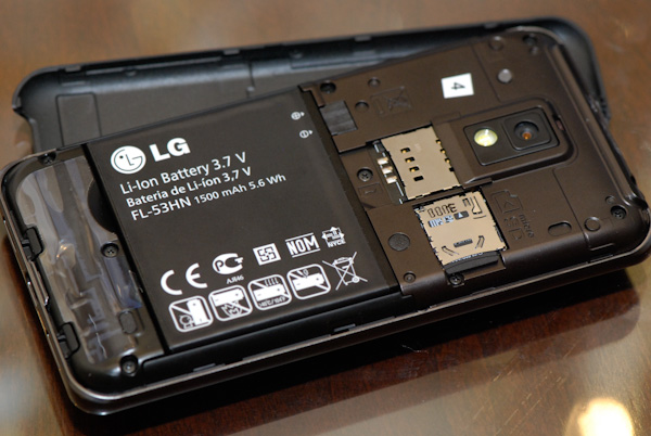
It’s been officially announced for some time now, but the LG Optimus 2X looks to be the first smartphone to include Nvidia’s Tegra 2 dual-core SoC. We’ve seen Tegra 2 in the ViewSonic G already, but this is the first time we’ve played with it in a real live smartphone. Suffice it to say the Optimus 2X is definitely impressive.
Final Words
Although it feels a bit odd to be talking about the same SoC architecture I did twelve months ago, the difference this time around is that NVIDIA actually has tangible design wins. LG’s Optimus 2X and Motorola’s ATRIX 4G both use NVIDIA’s Tegra 2 SoC and will be shipping later this quarter.
I’m also expecting to see a number of Froyo and Honeycomb based tablets running Tegra 2 to be teased at the show, although we probably won’t see them for an even longer period of time.
NVIDIA also managed some Tegra 2 design wins in automotive with announcements from Audi and Tesla at this year’s CES.
All in all, Tegra 2 is feeling a lot more like nForce 2 did upon its launch. It’s finally greeted with much better reception than its predecessor and it is poised to actually make some waves in the industry. Whether it can hold up to dual-core Snapdragon and TI’s OMAP 4 remains to be seen.
I believe we’ve probably seen NVIDIA’s best foot forward with Tegra 2 today, the question from here on out is one of execution and how soon can we get to the next iteration of the Tegra family.

