Original Link: https://www.anandtech.com/show/11839/intel-core-i9-7980xe-and-core-i9-7960x-review
The Intel Core i9-7980XE and Core i9-7960X CPU Review Part 1: Workstation
by Ian Cutress on September 25, 2017 3:01 AM EST
The buzz since Intel announced it was bringing an 18-core CPU to the consumer market has been palpable: users are anticipating this to be Intel’s best performing processor, and want to see it up against the 16-core AMD Threadripper (even at twice the cost). Intel is the incumbent: it has the legacy, the deep claws in software optimization, and the R&D clout to crush the red rival. However, a jump as large as this, moving from 10-core to 18-core in consumer, is a step Intel has been reluctant to make in the past. In this first analysis, we’ve run a few tests on the new 18-core (and 16-core) from Intel to find out the lie of the land.
Dissecting the new Core i9-7980XE and Core i9-7960X
Intel’s high-end desktop (HEDT) platform is designed to be the hard-hitting prosumer (professional consumer) platform providing all the cores without the extras required by the enterprise community. Up until this new generation of 2017 parts, we were treated to three or four CPUs each cycle, carved from Intel’s smallest enterprise silicon, slowly moving from 6 cores in 2009 to 10 cores in 2015, usually aiming for the top CPU to carve the $999 price point (usually at $999, anyway). With the 2017 HEDT platform, called Basin Falls, that changed.
The first launch of Basin Falls earlier this year had three parts. The new socket and chipset were expected as Intel updates every other generation, and this upgrade provided substantially more connectivity than before. The second part was the first three Skylake-X processors, built from Intel’s smallest enterprise silicon (like before), ranging from 6 cores at $389 to 10 cores at $999. Again, this second part was par for the course, albeit with a few microarchitecture changes in the design worth discussing (later). The third part of the initial launch was a bit of a curve ball: Intel configured two processors using their latest consumer microarchitecture, Kaby Lake-X. This is the curveball: normally the prosumer platform is a microarchitecture generation behind, due to development cycles. These two parts are also only quad-core, using repurposed ‘mainstream enthusiast’ parts but set at higher frequencies and higher power budgets, aiming to be the fastest single-threaded processors on the market.
The second launch of Basin Falls is basically what is happening today, and this is the new step from Intel. To add to the three Skylake-X processors already in the stack, using the smallest enterprise silicon, Intel is adding four more Skylake-X processors, this time using the middle-sized enterprise silicon. These new processors build on the others by significantly increasing core count, which comes at the cost of extra power requirements.
| Skylake-X Processors | ||||||||
| 7800X | 7820X | 7900X | 7920X | 7940X | 7960X | 7980XE | ||
| Silicon | LCC | HCC | ||||||
| Cores / Threads | 6/12 | 8/16 | 10/20 | 12/24 | 14/28 | 16/32 | 18/36 | |
| Base Clock / GHz | 3.5 | 3.6 | 3.3 | 2.9 | 3.1 | 2.8 | 2.6 | |
| Turbo Clock / GHz | 4.0 | 4.3 | 4.3 | 4.3 | 4.3 | 4.2 | 4.2 | |
| TurboMax Clock | N/A | 4.5 | 4.5 | 4.4 | 4.4 | 4.4 | 4.4 | |
| L3 | 1.375 MB/core | 1.375 MB/core | ||||||
| PCIe Lanes | 28 | 44 | 44 | |||||
| Memory Channels | 4 | 4 | ||||||
| Memory Freq DDR4 | 2400 | 2666 | 2666 | |||||
| TDP | 140W | 140W | 165W | |||||
| Price | $389 | $599 | $999 | $1199 | $1399 | $1699 | $1999 | |
All seven processors are listed in the table above. The four new parts are on the right, under the ‘HCC’ (high core count) silicon:
- The Core i9-7980XE, with 18 cores at $1999
- The Core i9-7960X, with 16 cores at $1699
- The Core i9-7940X, with 14 cores at $1399
- The Core i9-7920X, with 12 cores at $1199 (technically launched August 28th)
As with other product stacks, moving higher up step will cost more than the step previous. Intel (and others) are taking advantage of the fact that some consumers (and especially prosumers) will buy the best part because it can be offset against workflow, or just because it exists.
These four processors are almost identical, aside from core count: all four use the same base design, all four support DDR4-2666 memory out of the box, and all four will support 44 PCIe 3.0 lanes (plus 24 from the chipset). The top three are rated at 165W TDP (thermal design power), while the 12-core part is 140W. There is some variation in the frequencies: while all four parts will support 4.4 GHz as their top TurboMax clock (also known as ‘favored core’, more on this later), the Turbo 2.0 frequencies are all 4.3 GHz except the top two processors, and the base clock frequencies in general decrease the higher up the stack you go. This makes sense, physically: to keep the same TDP as cores are added, the processor will reduce in base clock frequency to meet that same target.
In our initial review of the Skylake-X processors, we were able to obtain the per-core turbo frequencies for each processor.
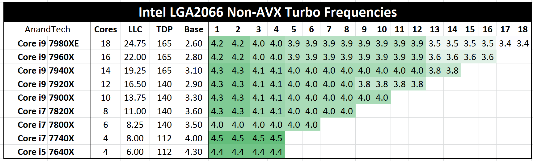
Despite the low base frequencies, each processor (when all cores are working) will still be above 3.4 GHz. The ‘base’ frequency number is essentially Intel’s guarantee: under normal conditions, this is the highest frequency Intel will guarantee. When AVX or AVX2/AVX512 instructions are being used, the frequencies will be lower than those listed (due to the energy density of these compact instructions) but still above the base frequency, and offering higher overall performance than using the same math in non-AVX formats.
Shown in the table are the turbo frequencies without TurboMax. TurboMax is a new feature first implemented with Broadwell-E, whereby the most efficient cores (as measured during manufacturing and embedded in the processor) can achieve a higher frequency. For Skylake-X, this feature was upgraded from one loaded core to when up to two cores are loaded. This means that the first two columns, labeled 1 and 2, will move up to 4.4 GHz for the top four processors. TurboMax also requires BIOS support, although we had some issues with this, mentioned later in this review.
Intel’s Competition: AMD
Before dissecting the processor, it is important to know what Intel is up against with the new processors. Arguably this is new territory for the consumer space: before this year, if a user wanted more than 10 cores, they had to invest in expensive Xeon processors (or even two of them), and a platform to support it.
Speaking directly for consumer lines, the obvious competition here is from AMD’s Threadripper processors. These are derived from their new Zen microarchitecture and offer 16-cores at $999 or 12 cores at $799.
| AMD vs Intel | ||||||||
| TR 1900X | TR 1920X | TR 1950X | 7920X | 7940X | 7960X | 7980XE | ||
| Silicon | 2 x Zeppelin | HCC | ||||||
| Cores / Threads | 8/16 | 12/24 | 16/32 | 12/24 | 14/28 | 16/32 | 18/36 | |
| Base Clock / GHz | 3.8 | 3.5 | 3.4 | 2.9 | 3.1 | 2.8 | 2.6 | |
| Turbo Clock / GHz | 4.0 | 4.0 | 4.0 | 4.3 | 4.3 | 4.2 | 4.2 | |
| XFR / TBM3 | 4.2 | 4.2 | 4.2 | 4.4 | 4.4 | 4.4 | 4.4 | |
| L2 | 512 KB/core | 1 MB/core | ||||||
| L3 | 32 MB | 64 MB | 1.375 MB/core | |||||
| PCIe Lanes | 60 | 44 | ||||||
| Memory Channels | 4 | 4 | ||||||
| Memory Freq DDR4 | 2666 | 2666 | ||||||
| TDP | 180W | 140W | 165W | |||||
| Price | $549 | $799 | $999 | $1199 | $1399 | $1699 | $1999 | |
From a performance perspective, Intel is expected to outright win: AMD’s 16-core processor was pitched against the previous generation’s 10-core processor and usually won, especially in multithreaded benchmarks. The single core performance of the AMD parts were a little behind Intel, but the core count made up for the difference. With Skylake-X adding both single thread performance as well as 8 more cores in the design should give Intel an easy lead in raw performance.
However, AMD has positioned that 1950X at $999, which is half the price of the i9-7980XE. AMD also cites more PCIe lanes from the CPU (60 vs 44), and no confusion over chipset functionality support. Intel’s rebuttal is that the performance is worth the cost, and that it has more chipset PCIe lanes for additional functionality beyond PCIe co-processors like GPUs.
Intel’s Competition: Intel
Intel’s enterprise Xeon platform is still a direct competitor here, in two different ways.
The ‘traditional’ multi-socket enterprise parts will cost substantially more than these new consumer parts, in exchange for some extra features as well, although even moving to a dual socket system with two $999 processors will not be much of a comparison: a Core i9-7980XE compared to a 2P Xeon Silver system will have advantages in core frequency and a unified memory interface, in exchange for maximum memory support and potential 10 gigabit Ethernet or Intel’s QuickAssist Technology.
| Ten+ Core Intel Xeon-W Processors (LGA2066) | |||||||
| Cores | Base Freq. |
Turbo 2.0 |
L3 (MB) |
L3/core (MB) |
TDP | Price | |
| Xeon W-2195 | 18/36 | 2.3 GHz | 4.3 GHz | 24.75 | 1.375 | 140 W | TBD |
| Xeon W-2175 | 14/28 | TBD | TBD | 19.25 | 1.375 | 140 W | TBD |
| Xeon W-2155 | 10/20 | 3.3 GHz | 4.5 GHz | 13.75 | 1.375 | 140 W | $1440 |
| Core i9-7980XE | 18/36 | 2.6 GHz | 4.2 GHz | 24.75 | 1.375 | 165W | $1999 |
| Core i9-7960X | 16/32 | 2.8 GHz | 4.2 GHz | 22.00 | 1.375 | 165W | $1699 |
Intel also launched Xeon-W processors in the last couple of weeks. These occupy the middle ground between Skylake-X and the enterprise Xeon-SP parts. Xeon-W uses the same socket as Skylake-X, but requires a completely new chipset, so the motherboards are not interchangeable. These Xeon-W parts are still up to 18 core, almost mirroring the Skylake-X processors, and support quad-channel memory, but support up to 512GB of ECC of it, compared to 128GB of non-ECC. The Xeon-W set of processors cost an extra 10-20% over the Skylake-X parts (add some more for the motherboard too), but for any prosumer that absolutely needs ECC memory, but does not want a dual-processor or does not have double the budget, then Xeon-W is going to be the best bet.
This Review: The Core i9-7980XE and Core i9-7960X
This review is titled ‘Part 1: Workstation’, as for the most part, this review will tackle some of the new processors in workstation type workloads including some initial data using SpecWPC, a standardized industry-standard workstation benchmark suite, as well as our more intense workloads. The review will take a nod towards usability with single-threaded workloads and responsiveness (because it really does matter how fast a PDF opens if this CPU is the main processor in a work system).
The main comparison points for this review will be AMD’s Ryzen Threadripper processors, the 16-core 1950X and the 12-core 1920X. On the Intel side, we retested the 10-core i7-6950X, as well as using our 10-core Core i9-7900X numbers from the initial Skylake review. Unfortunately we do not have the Core i9-7940X or Core i9-7920X yet to test, but we are working with Intel to get these parts in.
[Speaking directly from Ian]: I know a lot of our readers are gamers, and are interested in seeing how well (or poorly) these massive multi-core chips perform in the latest titles at the highest resolutions. Apologies to disappoint, but I am going to tackle the more traditional consumer tasks in a second review, and which will mean that gaming will be left for that review. For the users that have followed my reviews (and Twitter) of late, I am still having substantial issues with my X299 test beds on the gaming results, with Skylake-X massively underperforming where I would expect a much higher result. After having to dedicate recent time to business trips (Hot Chips, IFA) as well as other releases (Threadripper), I managed to sit down in the two weeks between trips to figure what exactly what was going on. I ended up throwing out the two X299 pre-launch engineering samples I was using for the Skylake-X testing, and I received a new retail motherboard only a few days before this review. This still has some issues that I spent time trying to debug, which I think are related to how the turbo is implemented, which could either be Intel related or BIOS-specific. To cause insult to injury to everyone who wants to see this data, I have jumped on a plane to travel half-way around the world for a business trip during the week of this launch, which leaves the current results inconclusive. I have reached out to the two other motherboard vendors that I haven’t received boards from; just in case the issue I seem to be having is vendor specific. If I ever find out what this issue is, then I will write it up, along with a full Skylake-X gaming suite. It will have to wait to mid-late October, due to other content (and more pre-booked event travel).
I also wanted to benchmark the EPYC CPUs that landed in my office a few days ago, but it was not immediately playing ball. I will have to try and get some Xeon-W / Xeon Gold for comparison with those.
Pages In This Review
- 1: Dissecting the Intel Core i9-7980XE and Core i9-7960X
- 2: New Features in Skylake-X: Cache, Mesh, and AVX-512
- 3: Explaining the Jump to HCC Silicon
- 4: Opinion: Why Counting ‘Platform’ PCIe Lanes (and using it in Marketing) Is Absurd
- 5: Test Bed and Setup
- 6: Benchmark Overview
- 7: Workstation Performance: SpecWPC v2.1
- 8: Benchmarking Performance: PCMark 10
- 9: Benchmarking Performance: Office Tests
- 10: Benchmarking Performance: Rendering Tests
- 11: Benchmarking Performance: Encoding Tests
- 12: Benchmarking Performance: System Tests
- 13: Benchmarking Performance: Legacy Tests
- 14: A Few Words on Power Consumption
- 15: Conclusions and Final Words
Related Reading
- The Intel Skylake-X Review: Core i9-7900X, i7-7820X and i7-7800X Tested
- The Intel Kaby Lake-X Review: Core i7-7740X and i5-7640X Tested
- Intel Announces Basin Falls: The New High-End Desktop Platform and X299 Chipset
New Features in Skylake-X: Cache, Mesh, and AVX-512
We have covered this in previous Skylake-X reviews, but it is worth a refresher about what is new in these Skylake-X processors over previous generations. The interesting thing to note is that the core design in these processors is different to the consumer-grade Skylake (known as Skylake-S) processors. This is a distinct change in policy from previous generations, where we saw parity on the base microarchitecture design. The changes for Skylake-X over Skylake-S are three fold: a change in the L2/L3 cache arrangement, a new routing mechanism for cores to send data, and the inclusion of AVX-512 units.
In our initial Skylake-X review, we tested how the new changes directly effect IPC / performance against Skylake-S in our benchmark suite. Overall they have a positive effect, with one major exception as noted below.
Cache Me If You Can: More Private L2 Cache
Modern Intel x86 processors use a three level cache design, known as L1, L2, and L3. The L1 cache is the one nearest to where the action happens in the processor core, so it is the fastest but also the smallest. When data is not in the L1 cache, a request is made to L2 cache, which is bigger but slightly slower. L3 follows the same route: bigger but slower. An ideal processor would have all of the data it needs always in the L1 cache in order to perform the best, but software is not always that nice: you cannot load that 4MB cat gif into a 1MB L2 cache.
In all of Intel’s Core microarchitecture designs, both the L1 and L2 caches are private to each core, with the L3 shared among all cores. This is achieved by giving each core a ‘slice’ of L3 cache and having appropriate tags, but allowing all the other cores to pull data from it when needed. The L3 level is typically where cores can ‘share’ data without going out to main memory (discussing simply here, rather than going into complex ideas such as snooping). In all previous Core designs, including Skylake-S, these caches were called inclusive caches: in each core, the L2 would contain a copy of L1, and the overriding L3 would contain a copy of every L2. This means that if a cache line in the L2 was invalidated, it would still be present in the L3 if needed later. This improves the ‘hit rate’ (getting data from a lower level cache), but puts demands on cache size: if a 10-core CPU has 10 L2 caches (one per core) at 256 KB each, the L3 cache must at least be 256 KB per core. Cache is not cheap and takes up a lot of die area, so it becomes a balance of performance and cost.
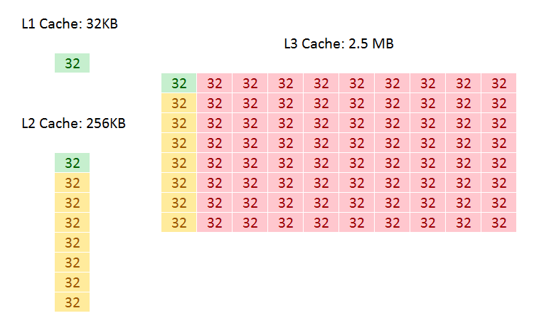
Inclusive Caches in Skylake-S: Green for L1 data, Yellow for L2 data, Red for L3 data
For Skylake-X, Intel does three things: it increases the size of the private L2 cache, which increases the hit rate for loading data, from 256 KB per core to 1 MB per core. To compensate for the increase in die area, Intel reduced the size of the size of the L3 from 2.5 MB per core to 1.375 MB per core, keeping the overall L2+L3 constant. The third element is inclusivity of the L3 cache: with it only being 1.375 MB per core, it no longer made sense for it to also hold 1 MB of the L2 data, and so with Skylake-X the L3 cache is now a non-inclusive cache (basically an exclusive cache) with the inability to obtain pre-fetch data from DRAM.
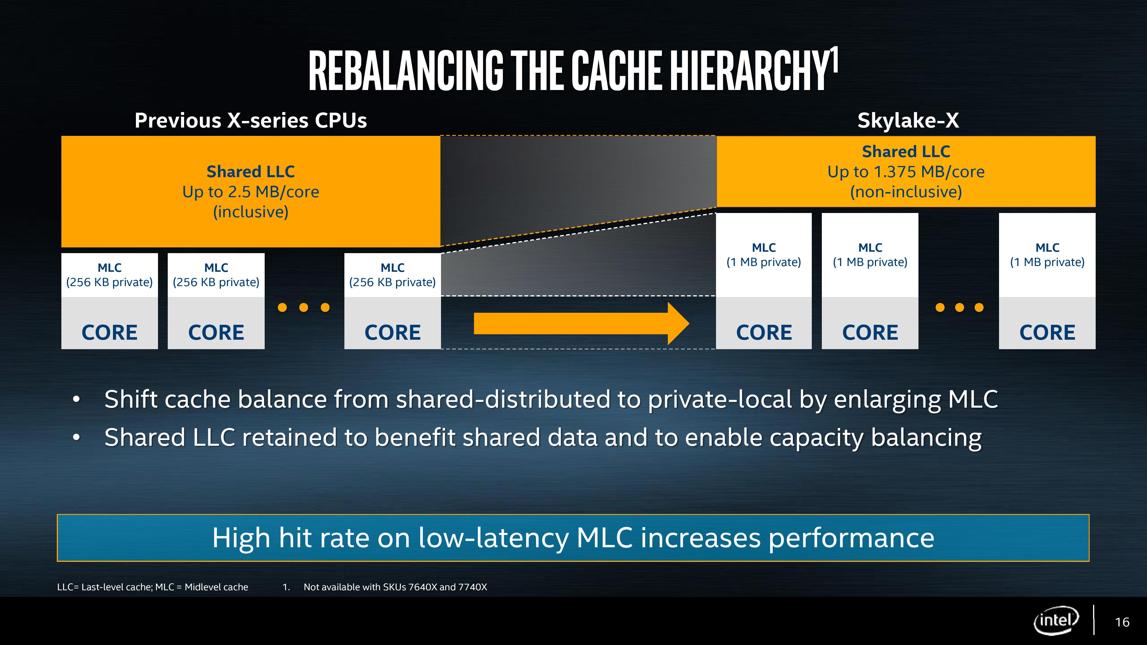
Moving the L3 to a non-inclusive cache with the inability to obtain data direct from DRAM turns it into what is known as a victim cache. When data comes in from DRAM into the L2, is used and then retired/overwritten, a copy is moved into the L3 (the L3 obtains the ‘victim’ cache line). If the data is then needed again in quick succession, there will be a copy in L3 rather than moving all the way out into DRAM. This situation depends highly on the software being used: software that has a large L2 cache requirement (e.g. 2MB) but frequency reuses data can take advantage of this scenario. Unfortunately not a lot of software is like this, and the L3 cache can become almost a dead-weight. Historically we see victim caches perform best with software that has a memory-speed bottleneck, or with integrated graphics. Skylake-X has no integrated graphics.
The upside is the size of the L2 private cache. Having spoken with engineers from different companies, a doubling of the size of the L2 cache often leads to a 1.414x decrease in cache misses (when data is not present and has to move out to the next level of cache). So by increasing the cache from 256 KB to 1 MB, thereby doubling the cache and doubling it again, the cache miss rate should be halved in total, leading to what most engineers would consider a 4-10% general IPC increase. The downside of a larger cache is that it takes longer to process data from it, adding latency. Keeping the latency low is difficult, but Intel claims that it has spent a lot of R&D effort here, with the L2 latency only moving from 11 cycles in Skylake-S to 13 cycles in Skylake-X. This will have a slight knock on that 4-10% IPC increase, but it does provide an overall benefit in almost all scenarios.
Making a Mesh: Replacing Rings with Routers
When reading about high performance processors, one phrase will always crop up: ‘feeding the beast’. In order for a CPU core to run at peak throughput, it has to continually have data to work on – if it does not have data to work on, it will sit idle and the throughput will drop. A lot of the core design is devoted to this problem: multi-level caches can store megabytes of data ready to go, and each generation brings a smarter pre-fetch engine to pull the right data from memory into cache at the right time. We’ve spoken about caches, but when a core needs data from the cache of another core, or needs to send/receive data from main memory, this also becomes a very important element to the design.
Most almost all of Intel’s processors, except for Xeon Phi, the solution to this problem has been bidirectional rings connecting the cores together (known as ring buses). The ring would allow data to travel in both directions, and it would have stations at each core (technically it grouped cores into pairs) as well as the main memory and system agent (IO). For the largest enterprise cores, in order to keep latency low, Intel separated the cores into two sets with some overlap, and a ring in each that had stations which could communicate with each other. As long as the cores and software kept the data it needed close by, latency was fairly low, and successive generations had led to higher frequencies and optimized design. The downside of a ring is scalability: the more cores you put in, the more variable the latency and more inconsistent performance can occur.

A dual ring design with Intel’s Xeon E5 v4 24-core processors
With Skylake-X, Intel felt that the ring strategy was not the right solution, and implemented its Xeon Phi strategy instead.
Rather than each core being a station on a ring, each core becomes a node in a two-dimensional grid or ‘mesh’. The node acts like a router: it is connected to the core above, the core below, and the core either side, and can direct data in each direction or drop it off at the core the node is on, similar to how a router works. In the scientific literature, this is seen as a decoupled crossbar (a central routing block), with the ‘decoupled’ bit being that every core acts like a localized crossbar.
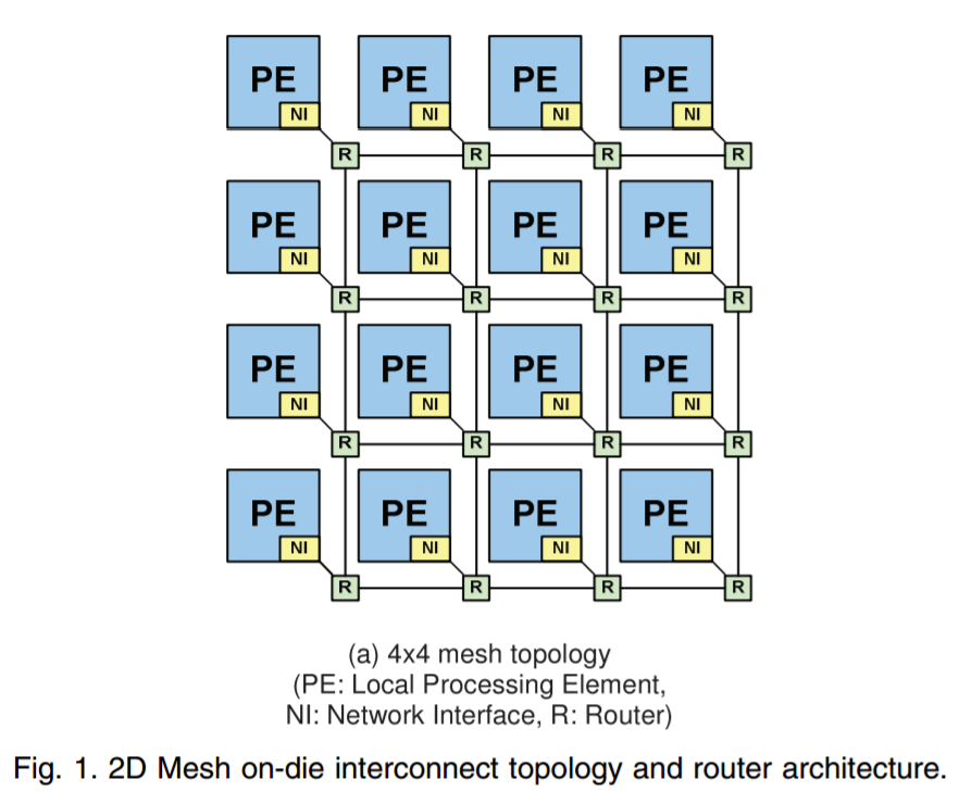
We believe that Intel is using a design known as MoDe-X, which simplifies the router at each stage to a very small routing mechanism, optimized through wiring lengths as these designs can burn power proportional to wire length. By optimizing in this way, Intel wants to reserve the power more for cores and IO. We go into greater depth on how MoDe-X works in our initial Skylake-X review.
So far the reaction to the mesh method has been mixed. While it offers scalability over using rings, it has not had over a decade of optimization, and some users have pointed to the frequency (usually 2.4 GHz) as being a bottleneck in their software over the faster ring design. Intel is likely to continue with the mesh design for the next few generations, so it will be interesting to see what upgrades are made (if disclosed).
I’ve Got 512 Problems but AVX Ain’t One: Accelerating Compute
Both the cache adjustment and the mesh networking are redesigns of features already implemented in the core. AVX-512 by contrast is a distinct addition to the design, requiring a fairly substantial amount of die area (approx. 20% of a Skylake-S core). Much like AVX and AVX2 before it, the point of AVX-512 is bundling sets of data together and performing the same operation on all the data with one instruction, rather than eight or sixteen instructions.
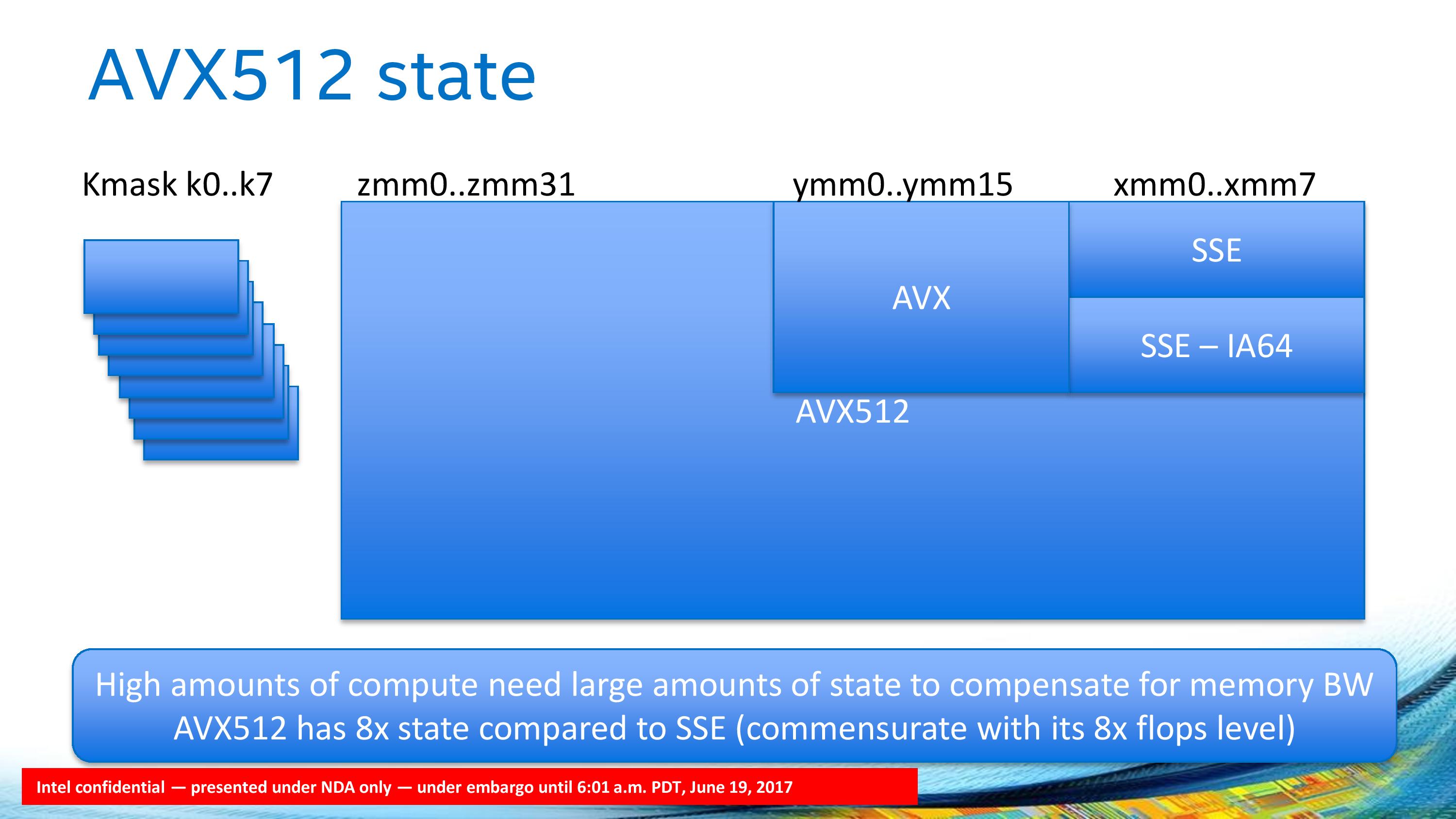
Bundling data together to unify a single instruction is at the heart of many dense compute tasks, and most prosumer and enterprise software with high compute requirements is designed with using instructions like this to accelerate performance. Most professional software today will take advantage of AVX or AVX2 instructions, with Intel expecting the same companies to update their software with AVX512 support soon.
Due to the density of the computation, the localized energy consumption is often very high (higher than in the standard core logic), and draws a lot of power – to compensate the core will often run at a lower frequency when these instructions are used, but there is an overall net gain. The support of AVX-512 is meant to be a highlight of Intel’s enterprise processors, but due to the unified design between enterprise and HEDT, consumers are able to take advantage as well, as long as their software does. For anyone using these new processors for light tasks, or gaming, are unlikely to see any advantage through AVX-512, announcing for a lot of unused silicon on the shiny new processor.
For the new processors launched today, all of them will support dual 512-bit FMA execution through a single 512-bit FMA on port 5, and a two joined 256-bit FMAs on ports 0 and 1. Intel had noted that the six and eight core parts on Skylake-X were manufactured with the port 5 FMA disabled, however several outlets have reported that both FMAs are detected for these parts.
There is a lot to dissect with AVX-512, such as the different instruction support as well as a few new (to Intel) implementations such as mask registers and small-datatype support. We covered this in detail in our initial Skylake-X review.
Explaining the Jump to Using HCC Silicon
When Intel makes its enterprise processors, it has historically produced three silicon designs:
- LCC: Low Core Count
- HCC: High Core Count (sometimes called MCC)
- XCC: Extreme Core Count (sometimes called HCC, to confuse)
The idea is that moving from LCC to XCC, the silicon will contain more cores (sometimes more features), and it becomes cost effective to have three different designs rather than one big one and disable parts to meet the range. The size of the LCC silicon is significantly smaller than the XCC silicon, allowing Intel to extract a better production cost per silicon die.
| Skylake-SP Die Sizes (from chip-architect.com) | |||
| Arrangement | Dimensions (mm) |
Die Area (mm2) |
|
| LCC | 3x4 (10-core) | 14.3 x 22.4 | 322 mm2 |
| HCC | 4x5 (18-core) | 21.6 x 22.4 | 484 mm2 |
| XCC | 5x6 (28-core) | 21.6 x 32.3 | 698 mm2 |
In the enterprise space, Intel has each of the three designs throughout its Xeon processor stack, ranging from four-core parts (usually cut down versions of the LCC silicon) all the way up to 28 core parts (using XCC) for this generation. The enterprise platform has more memory channels, support for error correcting and high-density memory, the ability to communicate to multiple processors, and several other RAS (reliability, accessibility, serviceability) features that are prominent for these markets. These are typically disabled for the prosumer platform.
In the past, Intel has only translated the LCC silicon into the prosumer platform. This was driven for a number of reasons.
- Cost: if users needed XCC, they had to pay the extra and Intel would not lose high-end sales.
- Software: Enterprise software is highly optimized for the core count, and systems are built especially for the customer. Prosumer software has to work on all platforms, and is typically not so multi-threaded.
- Performance: Large, multi-core silicon often runs at a low frequency to compensate. This can be suitable for an enterprise environment, but a prosumer environment requires responsiveness and users expect a good interactive experience.
- Platform Integration: Some large silicon might have additional design rules above and beyond the smaller silicon support, typically with power or features. In order to support this, a prosumer platform would require additional engineering/cost or lose flexibility.
So what changed at Intel in order to bring HCC silicon to the HEDT prosumer platform?
The short and shrift answer that many point to is AMD. This year AMD launched its own high-end desktop platform, based on its Ryzen Threadripper processors. With their new high performance core, putting up to 16 of them in a processor for $999 was somewhat unexpected, especially with the processor beating Intel’s top prosumer processors in some (not all) of the key industry benchmarks. The cynical might suggest that Intel had to move to the HCC strategy in order to stay at the top, even if their best processor will cost twice that of AMD.
Of course, transitioning a processor from the enterprise stack to the prosumer platform is not an overnight process, and many analysts have noted that it is likely that Intel has considered this option for several generations: testing it internally at least and looking at the market to decide when (or if) it is a good time to do so. The same analysts point to Intel’s initial lack of specifications aside from core count when these processors were first announced several months ago: specifications that would have historically been narrowed down at that point in previous designs if they were in the original plans. It is likely that the feasibly of introducing the HCC silicon was already in process, but actually moving that silicon to retail was a late addition to counter a threat to Intel’s top spot. That being said, to say Intel had never considered it would perhaps be a jump too far.
The question now becomes if the four areas listed above would all be suitable for prosumers and HEDT users:
- Cost: Moving the 18-core part into the $1999 is unprecedented for a consumer processor, so it will be interesting to see what the uptake will be. This does cut into Intel’s professional product line, where the equivalent processor is nearer $3500, but there are enough ‘cuts’ on the prosumer part for Intel to justify the difference: memory channels (4 vs 6), multi-processor support (1 vs 4), and ECC/RDIMM support (no vs yes). What the consumer platform does get in kind is overclocking support, which the enterprise platform does not.
- Software: Intel introduced its concept of ‘mega-tasking’ with the last generation HEDT platform, designed to encompass users and prosumers that use multiple software packages at once: encoding, streaming, content creation, emulation etc. Its argument now is that even if software cannot fully scale beyond a few cores, a user can either run multiple instances or several different software packages simultaneously without any slow-down. So the solution to this is rather a redefinition of the problem rather than anything else, which could have applied previously as well.
- Performance: Unlike enterprise processors, Intel is pushing the frequency on the new HCC parts for consumers. This translates into a slightly lower base frequency but a much higher turbo frequency, along with support for Turbo Max. In essence, software that requires responsiveness can still take advantage of the high frequency turbo modes, as long as the software is running solo. The disadvantage is going to be in power consumption, which is a topic later in the review.
- Platform Integration: Intel ‘solved’ this by creating one consumer platform suitable for nine processors with three different designs (Kaby Lake-X, Skylake-X LCC and Skylake-X HCC). Both the Kaby Lake-X and Skylake-X parts have different power delivery methods, support different numbers of memory channels, and different numbers of PCIe lanes / IO. When this was first announced, there was substantial commentary that this was making the platform overly complex, and would lead to confusion (it lead to at least one broken processor in our testing).
Each of these areas has either been marked as solved, or redefined out of being issue (even if a user agrees with the redefinition or not).
Opinion: Why Counting ‘Platform’ PCIe Lanes (and using it in Marketing) Is Absurd
It’s at this point that I’d like to take a detour and discuss something I’m not particularly happy with: counting PCIe lanes.
The number of PCIe lanes on a processor, for as long as I can remember, has always been about which lanes come directly from the PCIe root, offering full bandwidth and with the lowest possible latency. In modern systems this is the processor itself, or in earlier, less integrated systems, the Northbridge. By this metric, a standard Intel mainstream processor has 16 lanes, an AMD Ryzen has 16 or 20, an Intel HEDT processor has 28 or 44 depending on the model, and an AMD Ryzen Threadripper has 60.
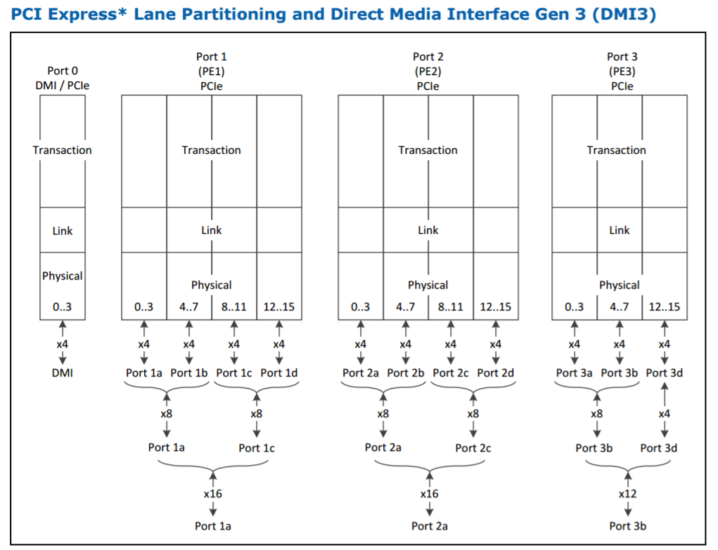
In Intel’s documentation, it explicitly lists what is available from the processor via the PCIe root complexes: here 44 lanes come from two lots of sixteen and one twelve lane complex. The DMI3 link to the chipset is in all but name a PCIe 3.0 x4 link, but is not included in this total.
The number of PCIe lanes on a chipset is a little different. Chipsets are for all practical purposes PCIe switches: using a limited bandwidth uplink, it is designed to carry traffic from low bandwidth controllers, such as SATA, Ethernet, and USB. AMD is limited in this regard, due to spending more time re-entering the pure CPU performance race over the last few years and outsource their designs to ASMedia. Intel has been increasing its PCIe 3.0 lane support on its chipsets for at least three generations, now supporting up to 24 PCIe 3.0 lanes. There are some caveats on what lanes can support which controllers, but in general we consider this 24.
Due to the shared uplink, PCIe lanes coming from the chipset (on both the AMD and Intel side) can be bottlenecked very easily, as well as being limited to PCIe 3.0 x4. The chipset introduces additional latency compared to having a controller directly attached to the processor, which is why we rarely see important hardware (GPUs, RAID controllers, FPGAs) connected to them.
The combination of the two lends itself to a variety of platform functionality and configurations. For example, for AMD's X399 platform that has 60 lanes from the processor, the following combinations are 'recommended':
| X399 Potential Configurations | |||
| Use | PCIe Lanes | Total | |
| Content Creator | 2 x Pro GPUs 2 x M.2 Cache Drives 10G Ethernet 1 x U.2 Storage 1 x M.2 OS/Apps 6 x SATA Local Backup |
x16/x16 from CPU x4 + x4 from CPU x4 from CPU x4 from CPU x4 from CPU From Chipset |
52 Lanes |
| Extreme PC | 2 x Gaming GPUs 1 x HDMI Capture Card 2 x M.2 for Games/Stream 10G Ethernet 1 x M.2 OS/Apps 6 x SATA Local Backup |
x16/x16 from CPU x8 from CPU x4 + x4 from CPU x4 from CPU x4 from CPU From Chipset |
56 Lanes |
| Streamer | 1 x Gaming GPU 1 x HDMI Capture Card 2 x M.2 Stream/Transcode 10G Ethernet 1 x U.2 Storage 1 x M.2 OS/Apps 6 x SATA Local Backup |
x16 from CPU x4 from CPU x4 + x4 from CPU x4 from CPU x4 from CPU x4 from CPU From Chipset |
40 Lanes |
| Render Farm | 4 x Vega FE Pro GPUs 2 x M.2 Cache Drives 1 x M.2 OS/Apps 6 x SATA Local Backup |
x16/x8/x8/x8 x4 + x4 from CPU x4 from CPU From Chipset |
52 Lanes |
What has started to happen is that these companies are combining both the CPU and chipset PCIe lane counts, in order to promote the biggest number. This is despite the fact that not all PCIe lanes are equal, they do not seem to care. As a result, Intel is cautiously promoting these new Skylake-X processors as having ’68 Platform PCIe lanes’, and has similar metrics in place for other upcoming hardware.
I want to nip this in the bud before it gets out of hand: this metric is misleading at best, and disingenuous at worst, especially given the history of how this metric has been provided in the past (and everyone will ignore the ‘Platform’ qualifier). Just because a number is bigger/smaller than a vendor expected does not give them the right to redefine it and mislead consumers.
To cite precedent: in the smartphone space, around 4-5 years ago, vendors were counting almost anything in the main processor as a core to provide a ‘full core count’. This meant that GPU segments became ‘cores’, special IP blocks for signal and image processing became ‘cores’, security IP blocks became ‘cores’. It was absurd to hear that a smartphone processor had fifteen cores, when the main general purpose cores were a quartet of ARM Cortex A7 designs. Users who follow the smartphone industry will notice that this nonsense stopped pretty quickly, partly due to anything being called a core, but some hints towards artificial cores potentially being placed in the system. If allowed to continue, this would have been a pointless metric.
The same thing is going to happen if the notion of ‘Platform PCIe Lanes’ is allowed to continue.
Test Bed and Setup
As per our processor testing policy, we take a premium category motherboard suitable for the socket, and equip the system with a suitable amount of memory running at the manufacturer's maximum supported frequency. This is also typically run at JEDEC subtimings where possible. It is noted that some users are not keen on this policy, stating that sometimes the maximum supported frequency is quite low, or faster memory is available at a similar price, or that the JEDEC speeds can be prohibitive for performance. While these comments make sense, ultimately very few users apply memory profiles (either XMP or other) as they require interaction with the BIOS, and most users will fall back on JEDEC supported speeds - this includes home users as well as industry who might want to shave off a cent or two from the cost or stay within the margins set by the manufacturer. Where possible, we will extend out testing to include faster memory modules either at the same time as the review or a later date.
| Test Setup | |
| Processor | Intel Core i9-7980XE (18C/36T, 165W, 2.6 GHz) Intel Core i9-7960X (16C/32T, 165W, 2.8 GHz) |
| Motherboards | GIGABYTE X299 Gaming 7 Pro |
| Cooling | Thermalright TRUE Copper |
| Power Supply | Corsair AX760i PSU Corsair AX1200i Platinum PSU |
| Memory | Corsair Vengeance Pro DDR4-2666 4x8 GB |
| Video Cards | MSI GTX 1080 Gaming 8GB ASUS GTX 1060 Strix Sapphire R9 Fury 4GB Sapphire RX 480 8GB Sapphire RX 460 2GB |
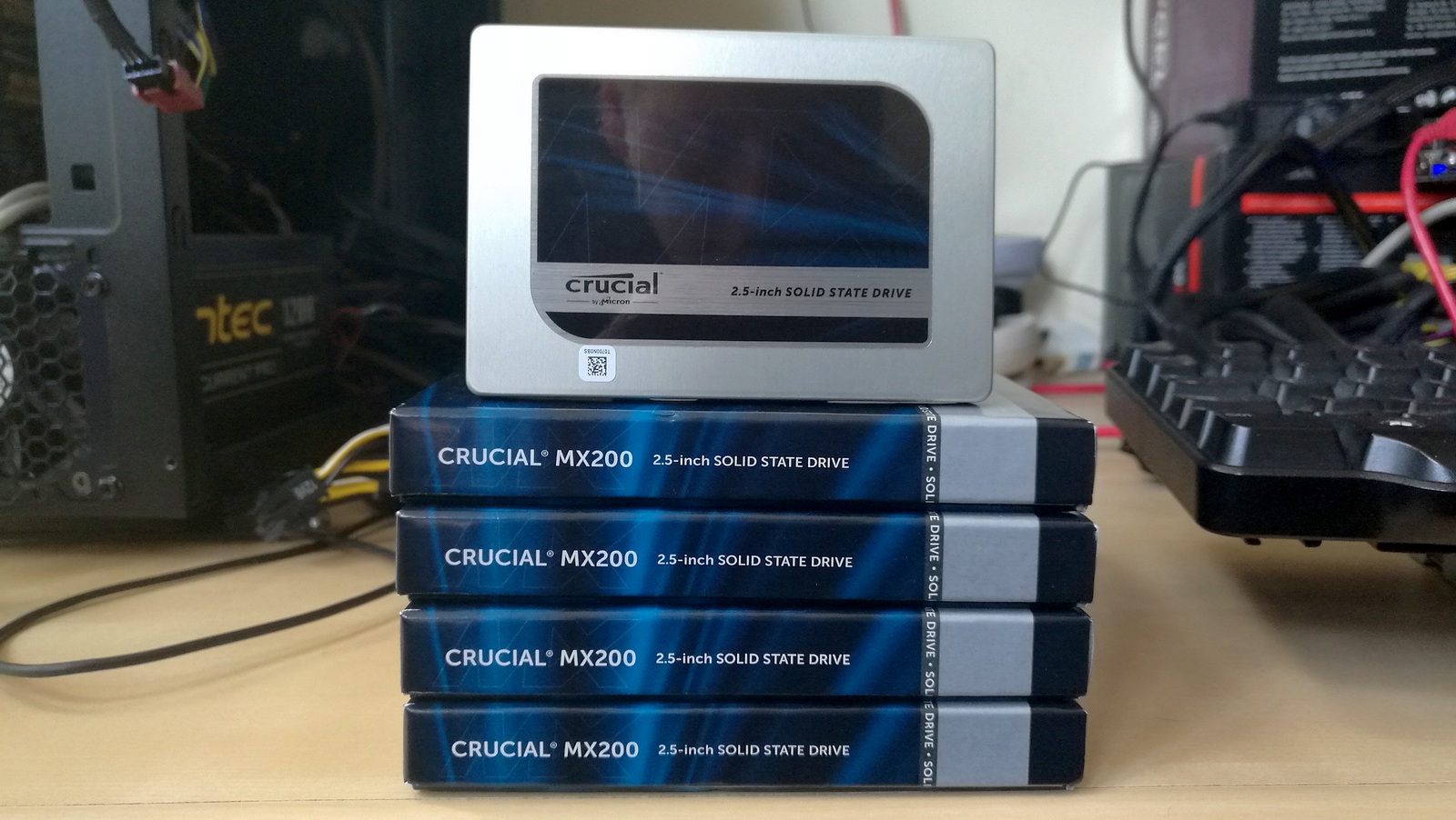
| Hard Drive | Crucial MX200 1TB |
| Optical Drive | LG GH22NS50 |
| Case | Open Test Bed |
| Operating System | Windows 10 Pro 64-bit |
Many thanks to...
We must thank the following companies for kindly providing hardware for our multiple test beds. Some of this hardware is not in this testbed specifically, but is used in other testing.
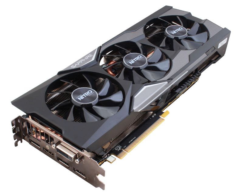
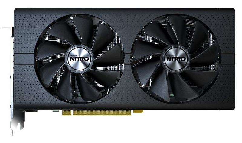
Thank you to Sapphire for providing us with several of their AMD GPUs. We met with Sapphire back at Computex 2016 and discussed a platform for our future testing on AMD GPUs with their hardware for several upcoming projects. As a result, they were able to sample us the latest silicon that AMD has to offer. At the top of the list was a pair of Sapphire Nitro R9 Fury 4GB GPUs, based on the first generation of HBM technology and AMD’s Fiji platform. As the first consumer GPU to use HDM, the R9 Fury is a key moment in graphics history, and these Nitro cards come with 3584 SPs running at 1050 MHz on the GPU with 4GB of 4096-bit HBM memory at 1000 MHz.
Further Reading: AnandTech’s Sapphire Nitro R9 Fury Review
Following the Fury, Sapphire also supplied a pair of their latest Nitro RX 480 8GB cards to represent AMD’s current performance silicon on 14nm (as of March 2017). The move to 14nm yielded significant power consumption improvements for AMD, which combined with the latest version of GCN helped bring the target of a VR-ready graphics card as close to $200 as possible. The Sapphire Nitro RX 480 8GB OC graphics card is designed to be a premium member of the RX 480 family, having a full set of 8GB of GDDR5 memory at 6 Gbps with 2304 SPs at 1208/1342 MHz engine clocks.
Further Reading: AnandTech’s AMD RX 480 Review
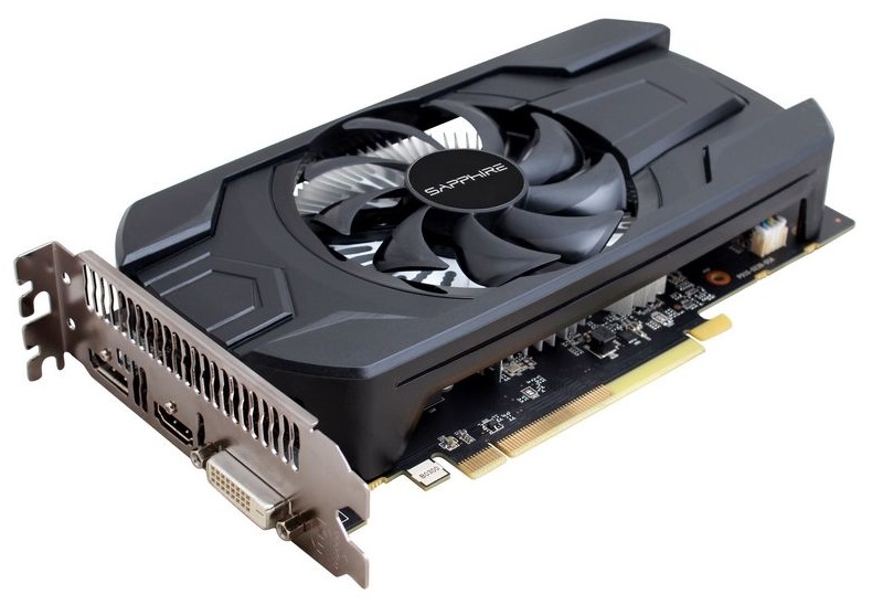
With the R9 Fury and RX 480 assigned to our gaming tests, Sapphire also passed on a pair of RX 460s to be used as our CPU testing cards. The amount of GPU power available can have a direct effect on CPU performance, especially if the CPU has to spend all its time dealing with the GPU display. The RX 460 is a nice card to have here, as it is powerful yet low on power consumption and does not require any additional power connectors. The Sapphire Nitro RX 460 2GB still follows on from the Nitro philosophy, and in this case is designed to provide power at a low price point. Its 896 SPs run at 1090/1216 MHz frequencies, and it is paired with 2GB of GDDR5 at an effective 7000 MHz.
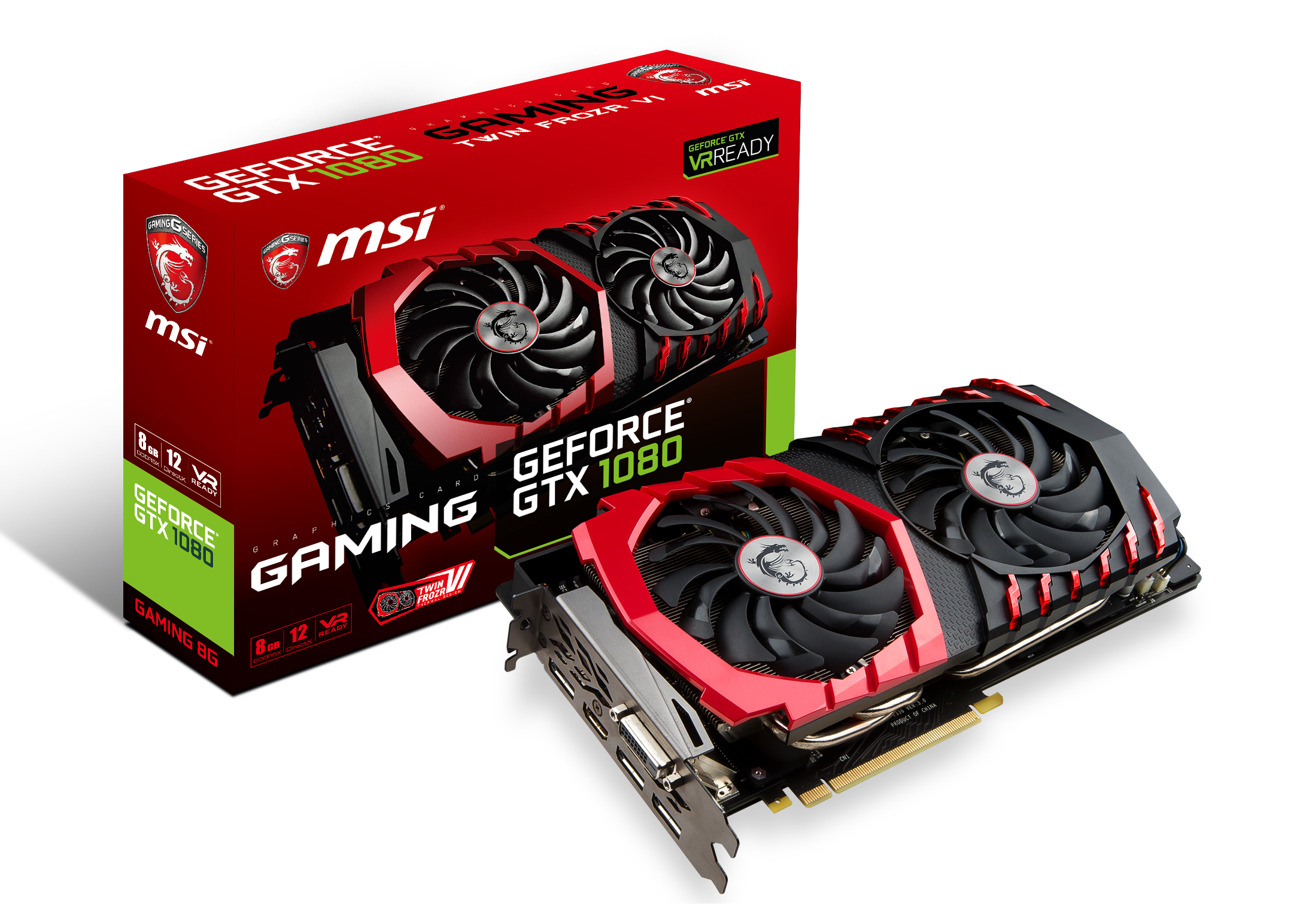
We must also say thank you to MSI for providing us with their GTX 1080 Gaming X 8GB GPUs. Despite the size of AnandTech, securing high-end graphics cards for CPU gaming tests is rather difficult. MSI stepped up to the plate in good fashion and high spirits with a pair of their high-end graphics. The MSI GTX 1080 Gaming X 8GB graphics card is their premium air cooled product, sitting below the water cooled Seahawk but above the Aero and Armor versions. The card is large with twin Torx fans, a custom PCB design, Zero-Frozr technology, enhanced PWM and a big backplate to assist with cooling. The card uses a GP104-400 silicon die from a 16nm TSMC process, contains 2560 CUDA cores, and can run up to 1847 MHz in OC mode (or 1607-1733 MHz in Silent mode). The memory interface is 8GB of GDDR5X, running at 10010 MHz. For a good amount of time, the GTX 1080 was the card at the king of the hill.
Further Reading: AnandTech’s NVIDIA GTX 1080 Founders Edition Review
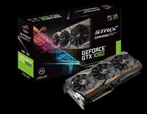
Thank you to ASUS for providing us with their GTX 1060 6GB Strix GPU. To complete the high/low cases for both AMD and NVIDIA GPUs, we looked towards the GTX 1060 6GB cards to balance price and performance while giving a hefty crack at >1080p gaming in a single graphics card. ASUS lended a hand here, supplying a Strix variant of the GTX 1060. This card is even longer than our GTX 1080, with three fans and LEDs crammed under the hood. STRIX is now ASUS’ lower cost gaming brand behind ROG, and the Strix 1060 sits at nearly half a 1080, with 1280 CUDA cores but running at 1506 MHz base frequency up to 1746 MHz in OC mode. The 6 GB of GDDR5 runs at a healthy 8008 MHz across a 192-bit memory interface.
Further Reading: AnandTech’s ASUS GTX 1060 6GB STRIX Review
Thank you to Crucial for providing us with MX200 SSDs. Crucial stepped up to the plate as our benchmark list grows larger with newer benchmarks and titles, and the 1TB MX200 units are strong performers. Based on Marvell's 88SS9189 controller and using Micron's 16nm 128Gbit MLC flash, these are 7mm high, 2.5-inch drives rated for 100K random read IOPs and 555/500 MB/s sequential read and write speeds. The 1TB models we are using here support TCG Opal 2.0 and IEEE-1667 (eDrive) encryption and have a 320TB rated endurance with a three-year warranty.
Further Reading: AnandTech's Crucial MX200 (250 GB, 500 GB & 1TB) Review
Thank you to Corsair for providing us with an AX1200i PSU. The AX1200i was the first power supply to offer digital control and management via Corsair's Link system, but under the hood it commands a 1200W rating at 50C with 80 PLUS Platinum certification. This allows for a minimum 89-92% efficiency at 115V and 90-94% at 230V. The AX1200i is completely modular, running the larger 200mm design, with a dual ball bearing 140mm fan to assist high-performance use. The AX1200i is designed to be a workhorse, with up to 8 PCIe connectors for suitable four-way GPU setups. The AX1200i also comes with a Zero RPM mode for the fan, which due to the design allows the fan to be switched off when the power supply is under 30% load.
Further Reading: AnandTech's Corsair AX1500i Power Supply Review
Thank you to G.Skill for providing us with memory. G.Skill has been a long-time supporter of AnandTech over the years, for testing beyond our CPU and motherboard memory reviews. We've reported on their high capacity and high-frequency kits, and every year at Computex G.Skill holds a world overclocking tournament with liquid nitrogen right on the show floor.
Further Reading: AnandTech's Memory Scaling on Haswell Review, with G.Skill DDR3-3000
Benchmark Overview
2017 CPU
For our review, we are implementing our fresh CPU testing benchmark suite, using new scripts developed specifically for this testing. This means that with a fresh OS install, we can configure the OS to be more consistent, install the new benchmarks, maintain software version consistency without random updates and start running the tests in under 5 minutes. After that it's a one button press to start an 8-10hr test (with a high-performance core) with nearly 100 relevant data points in the benchmarks given below. The tests cover a wide range of segments, some of which will be familiar but some of the tests are new to benchmarking in general, but still highly relevant for the markets they come from.
Our new CPU tests go through six main areas. We cover the Web (we've got an un-updateable version of Chrome 56), general system tests (opening tricky PDFs, emulation, brain simulation, AI, 2D image to 3D model conversion), rendering (ray tracing, modeling), encoding (compression, AES, h264 and HEVC), office based tests (PCMark and others), and our legacy tests, throwbacks from another generation of bad code but interesting to compare.
All of our benchmark results can also be found in our benchmark engine, Bench.
A side note on OS preparation. As we're using Windows 10, there's a large opportunity for something to come in and disrupt our testing. So our default strategy is multiple: disable the ability to update as much as possible, disable Windows Defender, uninstall OneDrive, disable Cortana as much as possible, implement the high performance mode in the power options, and disable the internal platform clock which can drift away from being accurate if the base frequency drifts (and thus the timing ends up inaccurate).
New Tests
SpecWPC v2.1 – A lot of the industry turn to SPEC to produce standard benchmarks suitable for various markets. The latest version of the workstation focused benchmark suite was released this year, and tackles six main areas with over 30 different benchmarks. These include compute, visualization, medical, oil and gas, finance, and typical workstation areas. For consistency we run all the tests (except IOMeter) on Windows 10, using an RX 460 graphics card at 1080p resolution with an MX200 SSD.
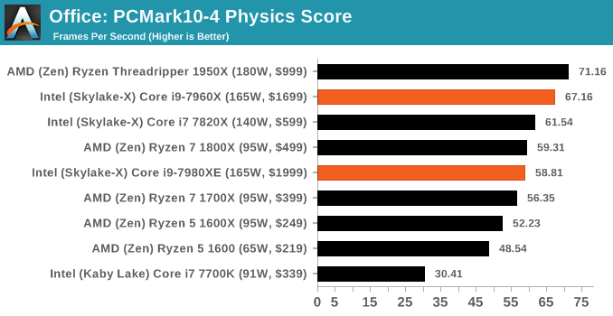
PCMark10 – We had several requests to include PCMark10 in our new testing suite. Normally we wait until a new benchmark has most of the problems ironed out, however our initial performance scaling metrics show that PCMark10 is basically there already. The extended suite covers ‘Essential, Productivity and Creativity’ benchmarks such as GIMP, Blender, video editing, conferencing, complex spreadsheets and other tests. We use the subtest values as well as the gaming physics result.
Agisoft PhotoScan 1.3.3 – Again, requests to use a more updated version of Photoscan were also coming through the inbox. Over the older version, Photoscan includes various throughput enhancements to each of the core points of the algorithm. Agisoft also gave us a new larger set of more detailed test images to generate our 3D models, giving a longer benchmark (but results are not comparable to the old data). We’ve run this benchmark on about a dozen CPUs ready for this review.
Office / Professional Tests
PCMark8
Chromium Compile (v56)
Rendering Tests
Corona 1.3
Blender 2.78
LuxMark v3.1 CPU C++
LuxMark v3.1 CPU OpenCL
POV-Ray 3.7.1b4
Cinebench R15 ST
Cinebench R15 MT
Encoding Tests
7-Zip 9.2
WinRAR 5.40
AES Encoding (TrueCrypt 7.2)
HandBrake v1.0.2 x264 LQ
HandBrake v1.0.2 x264-HQ
HandBrake v1.0.2 HEVC-4K
System Tests
PDF Opening
FCAT
3DPM v2.1
Dolphin v5.0
DigiCortex v1.20
Agisoft PhotoScan v1.0
Legacy Tests
3DPM v1 ST / MT
x264 HD 3 Pass 1, Pass 2
Cinebench R11.5 ST / MT
Cinebench R10 ST / MT
A Note on CPU Gaming Tests (Repeat from Page 1)
I know a lot of our readers are gamers, and are interested in seeing how well (or poorly) these massive multi-core chips perform in the latest titles at the highest resolutions. Apologies to disappoint, but I am going to tackle the more traditional consumer tasks in a second review, and which will mean that gaming will be left for that review. For the users that have followed my reviews (and Twitter) of late, I am still having substantial issues with my X299 test beds on the gaming results, with Skylake-X massively underperforming where I would expect a much higher result.
After having to dedicate recent time to business trips (Hot Chips, IFA) as well as other releases (Threadripper), I managed to sit down in the two weeks between trips to figure what exactly what was going on. I ended up throwing out the two X299 pre-launch engineering samples I was using for the Skylake-X testing, and I received a new retail motherboard only a few days before this review. This still has some issues that I spent time trying to debug, which I think are related to how turbo is implemented, which could either be Intel related or BIOS specific.
To cause insult to injury to everyone who wants to see this data, I have jumped on a plane to travel half-way around the world for a business trip during the week of this launch, which leaves the current results inconclusive. I have reached out to the two other motherboard vendors that I haven’t received boards from; just in case the issue I seem to be having is vendor specific. If I ever find out what this issue is, then I will write it up, along with a full Skylake-X gaming suite. It will have to wait to mid-late October, due to other content (and more pre-booked event travel).
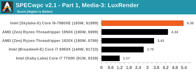
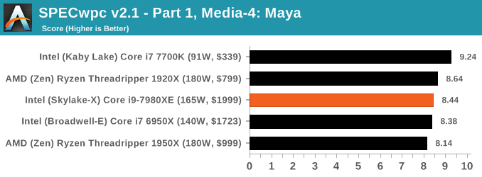
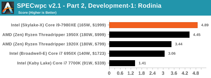
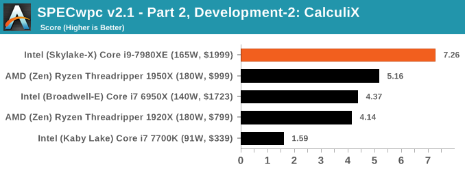
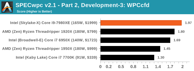
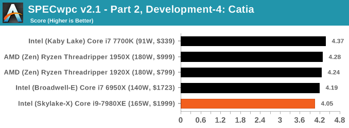
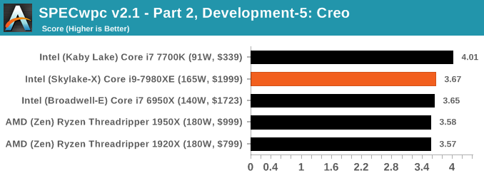
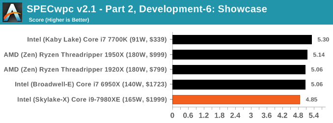
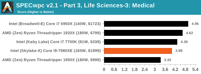
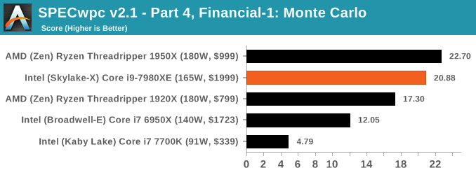
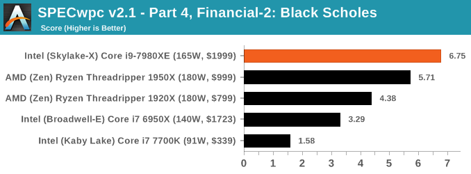
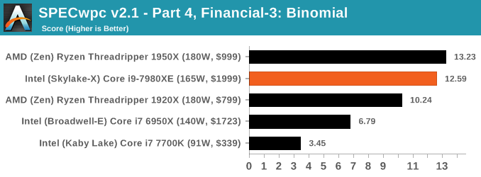
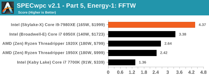
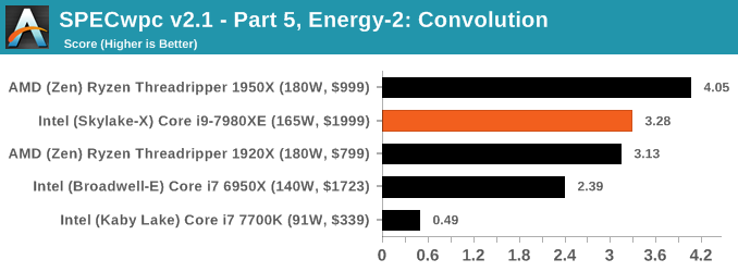
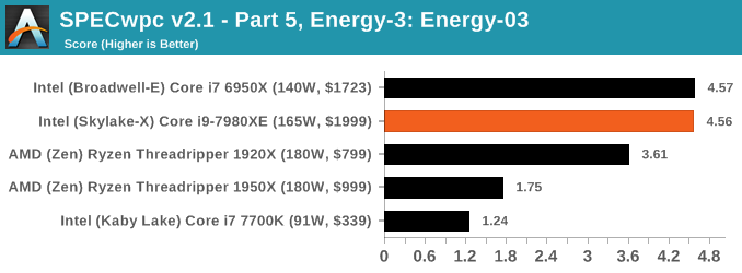
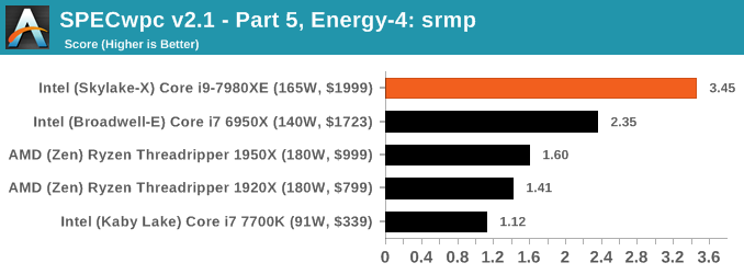
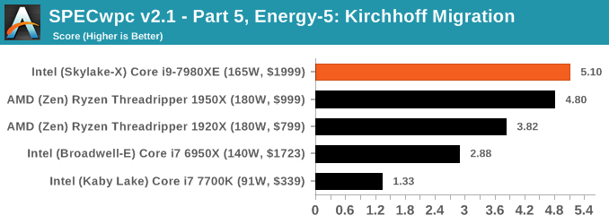
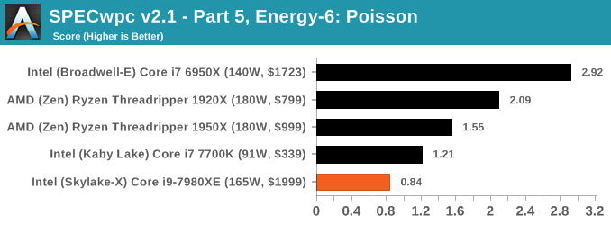
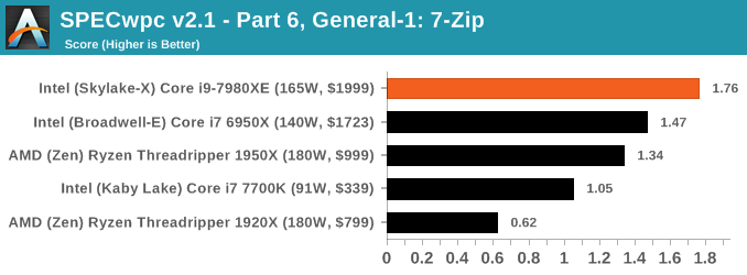
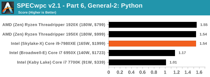
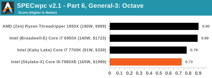
Benchmarking Performance: SPECwpc v2.1
Anyone can run wPrime (why would you?) or Geekbench, but more often than not these pre-built synthetic tests are not representative of any user’s workload. This applies even more to professional environments or prosumer workloads, where time is money: if someone interested in hardware cannot pinpoint exactly how the new hardware is going to benefit them, that is $20 of billable time down the drain.
One of the difficulties of a benchmark reviewer is finding relevant benchmarks for the audience at hand. I’ve discussed what AnandTech is and our audience to several high profile software vendors who are in the business of supplying professional grade, critical programs that top technology companies use to produce the next $700 smartphone. These engineers are our readers, and it only seems best that we benchmark something that can assist them in accelerating our workflow. Unfortunately, the almost blanket response from these ISVs is negative, even if the request is for a limited software license in exchange for repeated discussion of the software on AnandTech (and third party benchmark data to assist their customers in hardware purchasing). My last discussions with two major ISVs led to a ‘interesting but we don’t see the value’ response and a ‘we’re doing our own in-house thing’ response respectively. No-one wants to know. Unless you work at one of these companies and want to get in touch.
The fall-back position in this case is to call on SPEC for their Workstation benchmark series. SPECwpc has existed in one form or another for several years, using pre-compiled binaries for a mix of medical, oil-and-gas, engineering, visualization and system level benchmarks. There are over 30 benchmarks, some running multiple copies to keep all the cores busy, and repeated runs offer very good consistency. A full run can take over six hours, making a sizeable increase to even our CPU workflow.
We’re reporting almost all of the subset scores in our benchmarking. Some tests require a GPU, and so we maintain the same RX 460 graphics card on each processor we test, along with the same screen resolution and driver. Ideally we would use professional graphics cards, like AMD’s FirePro range or NVIDIA’s Quadro range, however we currently use four identical RX 460 cards to keep the benchmarks on our test beds continually flowing, and sourcing four of the same pro card on long-term loan is actually fairly difficult.
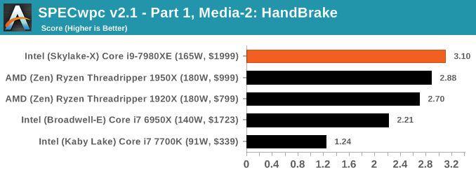
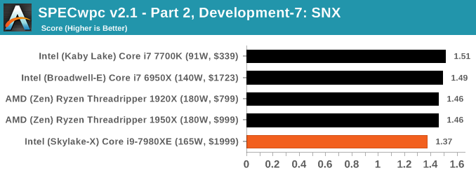
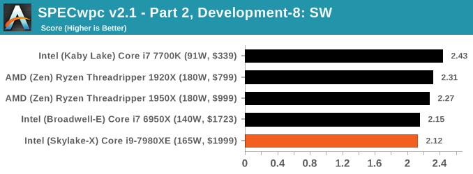
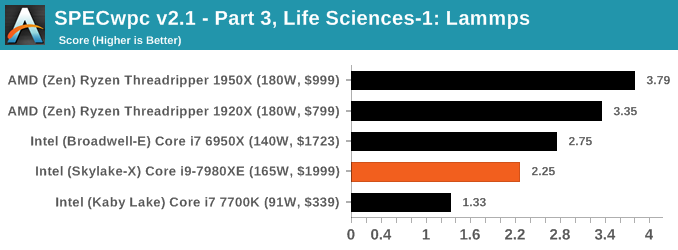
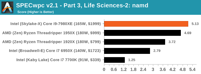
Because SPECwpc takes so long and is fairly new, we only have results for a few processors so far. This should expand as we continue using this test. We’re likely to limit this test to HEDT processors and above, along with one or two mainstream processors (i7-K, Ryzen 7). For this review, out of the two Intel processors in the title, we only had time to run it on the Core i9-7980XE.
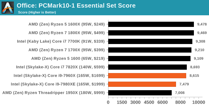
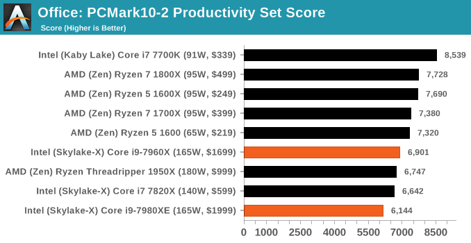
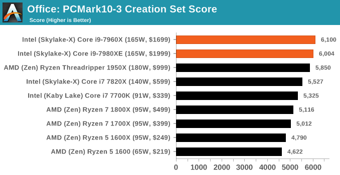
Benchmarking Performance: PCMark 10
PCMark 10 is the 2017 update to the family favorite, PCMark 8. PCMark 8 has been part of our test bed since the latest update in Q1. For the most part it runs well, although for some processors it doesn’t recognize, some tests will not complete, leading to holes in our benchmark data (there’s also an odd directory quirk in one test that causes issues). The newest version, PCMark 10, is the answer.
The new test is adapted for more 2016/2017 workflows. With the advent of office applications that perform deeper compute tasks, or the wave of online gamers and streamers, the idea behind PCMark 10 is to give a better ‘single number’ result that can provide a comparable metric between systems. Single metrics never tell the whole story, so we’re glad that Futuremark provides a very detailed breakdown of what goes on.
Ganesh’s article on PCMark 10 goes into more detail than I will here, but the ‘Extended Benchmark’ runs through four different sets of tests: Essential, Productivity, Creation and Gaming. Each of these have sub-test results as well, including startup performance, web performance, video conferencing, photo/video editing, spreadsheets, rendering, and physics, which you can find in Bench.
Benchmarking Performance: CPU Office Tests
The office programs we use for benchmarking aren't specific programs per-se, but industry standard tests that hold weight with professionals. The goal of these tests is to use an array of software and techniques that a typical office user might encounter, such as video conferencing, document editing, architectural modelling, and so on and so forth.
All of our benchmark results can also be found in our benchmark engine, Bench.
Chromium Compile (v56)
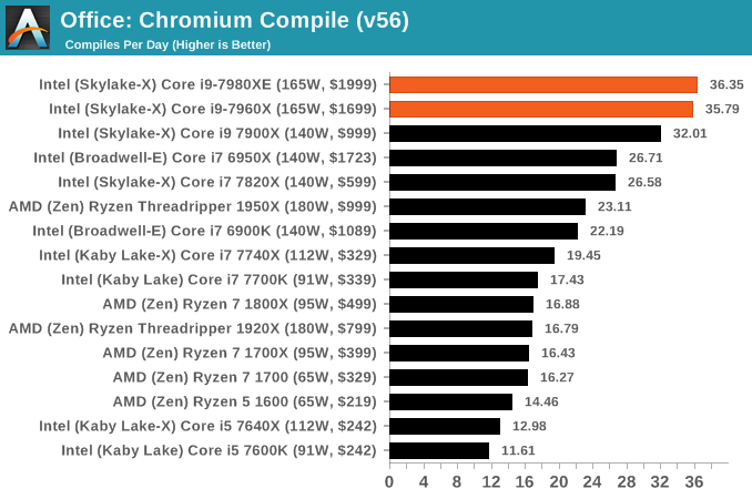
Our new compilation test uses Windows 10 Pro, VS Community 2015.3 with the Win10 SDK to combile a nightly build of Chromium. We've fixed the test for a build in late March 2017, and we run a fresh full compile in our test. Compilation is the typical example given of a variable threaded workload - some of the compile and linking is linear, whereas other parts are multithreaded.
PCMark8: link
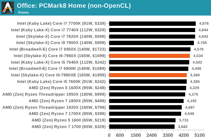
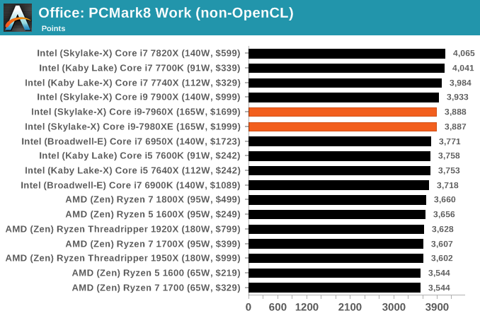
Despite originally coming out in 2008/2009, Futuremark has maintained PCMark8 to remain relevant in 2017. On the scale of complicated tasks, PCMark focuses more on the low-to-mid range of professional workloads, making it a good indicator for what people consider 'office' work. We run the benchmark from the commandline in 'conventional' mode, meaning C++ over OpenCL, to remove the graphics card from the equation and focus purely on the CPU. PCMark8 offers Home, Work and Creative workloads, with some software tests shared and others unique to each benchmark set.
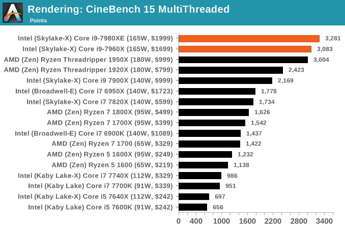
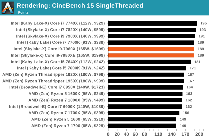
Benchmarking Performance: CPU Rendering Tests
Rendering tests are a long-time favorite of reviewers and benchmarkers, as the code used by rendering packages is usually highly optimized to squeeze every little bit of performance out. Sometimes rendering programs end up being heavily memory dependent as well - when you have that many threads flying about with a ton of data, having low latency memory can be key to everything. Here we take a few of the usual rendering packages under Windows 10, as well as a few new interesting benchmarks.
All of our benchmark results can also be found in our benchmark engine, Bench.
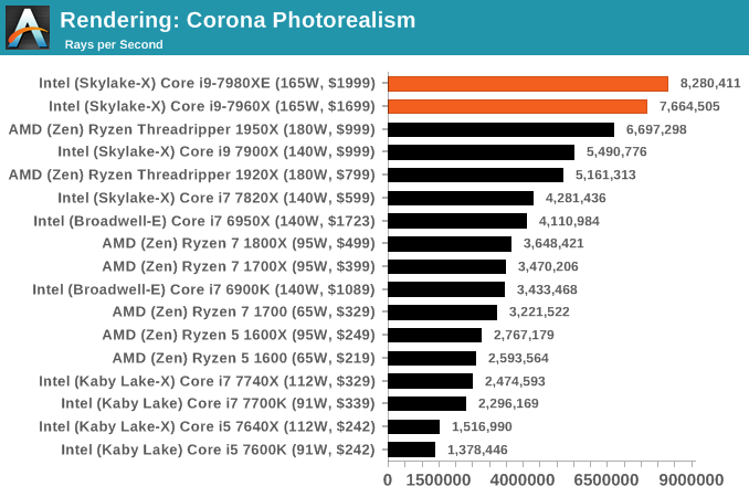
Corona 1.3: link
Corona is a standalone package designed to assist software like 3ds Max and Maya with photorealism via ray tracing. It's simple - shoot rays, get pixels. OK, it's more complicated than that, but the benchmark renders a fixed scene six times and offers results in terms of time and rays per second. The official benchmark tables list user submitted results in terms of time, however I feel rays per second is a better metric (in general, scores where higher is better seem to be easier to explain anyway). Corona likes to pile on the threads, so the results end up being very staggered based on thread count.
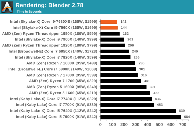
Blender 2.78: link
For a render that has been around for what seems like ages, Blender is still a highly popular tool. We managed to wrap up a standard workload into the February 5 nightly build of Blender and measure the time it takes to render the first frame of the scene. Being one of the bigger open source tools out there, it means both AMD and Intel work actively to help improve the codebase, for better or for worse on their own/each other's microarchitecture.
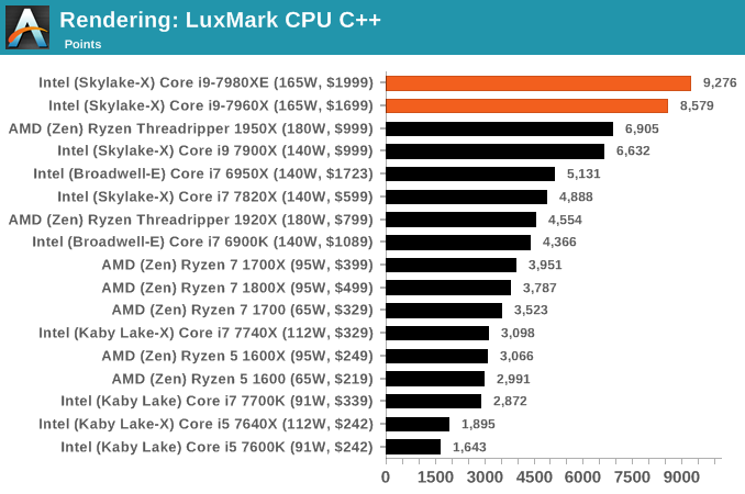
LuxMark v3.1: Link
As a synthetic, LuxMark might come across as somewhat arbitrary as a renderer, given that it's mainly used to test GPUs, but it does offer both an OpenCL and a standard C++ mode. In this instance, aside from seeing the comparison in each coding mode for cores and IPC, we also get to see the difference in performance moving from a C++ based code-stack to an OpenCL one with a CPU as the main host.
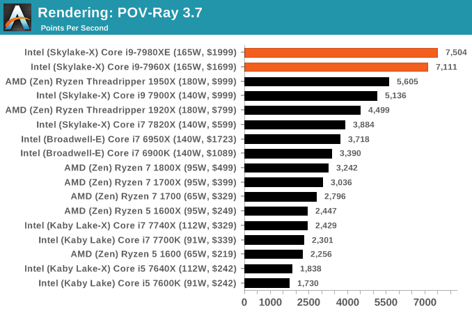
POV-Ray 3.7.1b4: link
Another regular benchmark in most suites, POV-Ray is another ray-tracer but has been around for many years. It just so happens that during the run up to AMD's Ryzen launch, the code base started to get active again with developers making changes to the code and pushing out updates. Our version and benchmarking started just before that was happening, but given time we will see where the POV-Ray code ends up and adjust in due course.
Cinebench R15: link
The latest version of CineBench has also become one of those 'used everywhere' benchmarks, particularly as an indicator of single thread performance. High IPC and high frequency gives performance in ST, whereas having good scaling and many cores is where the MT test wins out.
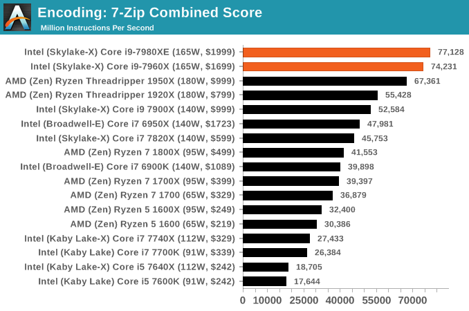
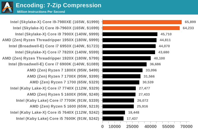
Benchmarking Performance: CPU Encoding Tests
One of the interesting elements on modern processors is encoding performance. This includes encryption/decryption, as well as video transcoding from one video format to another. In the encrypt/decrypt scenario, this remains pertinent to on-the-fly encryption of sensitive data - a process by which more modern devices are leaning to for software security. Video transcoding as a tool to adjust the quality, file size and resolution of a video file has boomed in recent years, such as providing the optimum video for devices before consumption, or for game streamers who are wanting to upload the output from their video camera in real-time. As we move into live 3D video, this task will only get more strenuous, and it turns out that the performance of certain algorithms is a function of the input/output of the content.
All of our benchmark results can also be found in our benchmark engine, Bench.
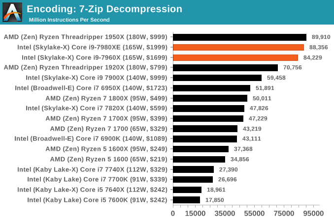
7-Zip 9.2: link
One of the freeware compression tools that offers good scaling performance between processors is 7-Zip. It runs under an open-source licence, is fast, and easy to use tool for power users. We run the benchmark mode via the command line for four loops and take the output score.
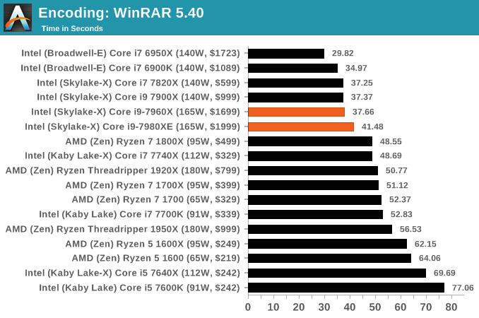
WinRAR 5.40: link
For the 2017 test suite, we move to the latest version of WinRAR in our compression test. WinRAR in some quarters is more user friendly that 7-Zip, hence its inclusion. Rather than use a benchmark mode as we did with 7-Zip, here we take a set of files representative of a generic stack (33 video files in 1.37 GB, 2834 smaller website files in 370 folders in 150 MB) of compressible and incompressible formats. The results shown are the time taken to encode the file. Due to DRAM caching, we run the test 10 times and take the average of the last five runs when the benchmark is in a steady state.
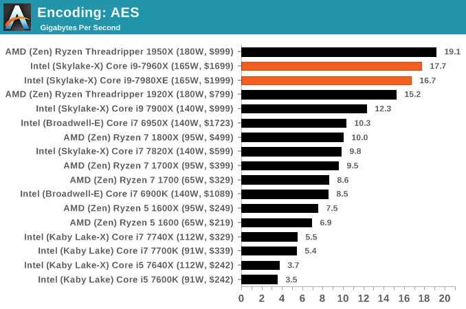
AES Encoding
Algorithms using AES coding have spread far and wide as a ubiquitous tool for encryption. Again, this is another CPU limited test, and modern CPUs have special AES pathways to accelerate their performance. We often see scaling in both frequency and cores with this benchmark. We use the latest version of TrueCrypt and run its benchmark mode over 1GB of in-DRAM data. Results shown are the GB/s average of encryption and decryption.
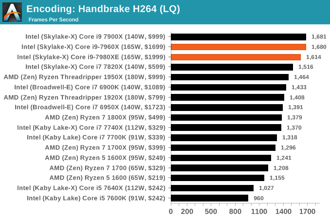
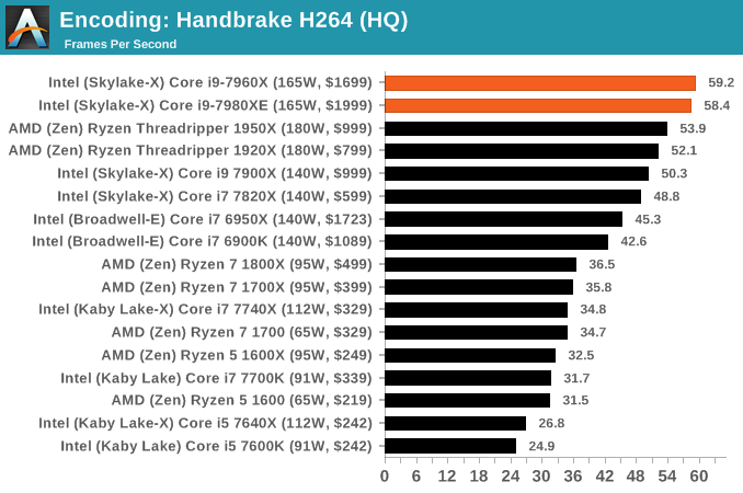
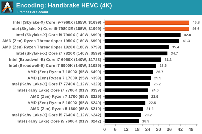
HandBrake v1.0.2 H264 and HEVC: link
As mentioned above, video transcoding (both encode and decode) is a hot topic in performance metrics as more and more content is being created. First consideration is the standard in which the video is encoded, which can be lossless or lossy, trade performance for file-size, trade quality for file-size, or all of the above can increase encoding rates to help accelerate decoding rates. Alongside Google's favorite codec, VP9, there are two others that are taking hold: H264, the older codec, is practically everywhere and is designed to be optimized for 1080p video, and HEVC (or H265) that is aimed to provide the same quality as H264 but at a lower file-size (or better quality for the same size). HEVC is important as 4K is streamed over the air, meaning less bits need to be transferred for the same quality content.
Handbrake is a favored tool for transcoding, and so our test regime takes care of three areas.
Low Quality/Resolution H264: Here we transcode a 640x266 H264 rip of a 2 hour film, and change the encoding from Main profile to High profile, using the very-fast preset.
High Quality/Resolution H264: A similar test, but this time we take a ten-minute double 4K (3840x4320) file running at 60 Hz and transcode from Main to High, using the very-fast preset.
HEVC Test: Using the same video in HQ, we change the resolution and codec of the original video from 4K60 in H264 into 4K60 HEVC.
Benchmarking Performance: CPU System Tests
Our first set of tests is our general system tests. These set of tests are meant to emulate more about what people usually do on a system, like opening large files or processing small stacks of data. This is a bit different to our office testing, which uses more industry standard benchmarks, and a few of the benchmarks here are relatively new and different.
All of our benchmark results can also be found in our benchmark engine, Bench.
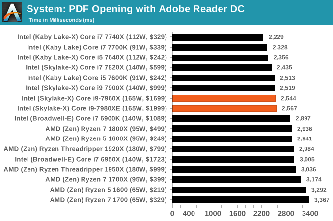
PDF Opening
First up is a self-penned test using a monstrous PDF we once received in advance of attending an event. While the PDF was only a single page, it had so many high-quality layers embedded it was taking north of 15 seconds to open and to gain control on the mid-range notebook I was using at the time. This put it as a great candidate for our 'let's open an obnoxious PDF' test. Here we use Adobe Reader DC, and disable all the update functionality within. The benchmark sets the screen to 1080p, opens the PDF to in fit-to-screen mode, and measures the time from sending the command to open the PDF until it is fully displayed and the user can take control of the software again. The test is repeated ten times, and the average time taken. Results are in milliseconds.
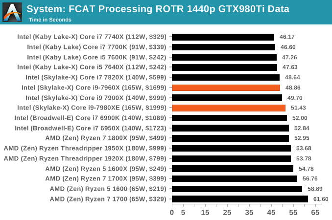
FCAT Processing: link
One of the more interesting workloads that has crossed our desks in recent quarters is FCAT - the tool we use to measure stuttering in gaming due to dropped or runt frames. The FCAT process requires enabling a color-based overlay onto a game, recording the gameplay, and then parsing the video file through the analysis software. The software is mostly single-threaded, however because the video is basically in a raw format, the file size is large and requires moving a lot of data around. For our test, we take a 90-second clip of the Rise of the Tomb Raider benchmark running on a GTX 980 Ti at 1440p, which comes in around 21 GB, and measure the time it takes to process through the visual analysis tool.
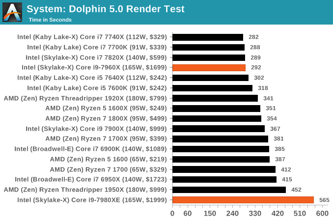
Dolphin Benchmark: link
Many emulators are often bound by single thread CPU performance, and general reports tended to suggest that Haswell provided a significant boost to emulator performance. This benchmark runs a Wii program that ray traces a complex 3D scene inside the Dolphin Wii emulator. Performance on this benchmark is a good proxy of the speed of Dolphin CPU emulation, which is an intensive single core task using most aspects of a CPU. Results are given in minutes, where the Wii itself scores 17.53 minutes.
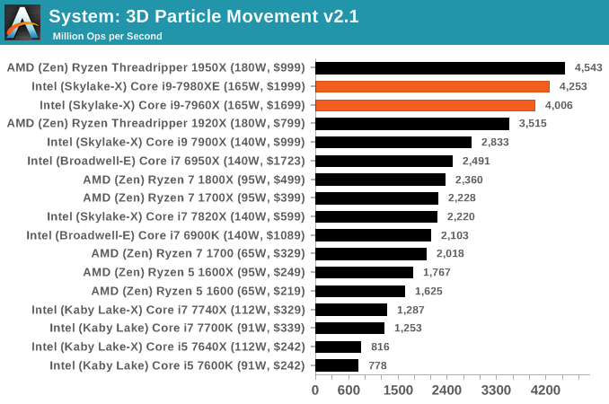
3D Movement Algorithm Test v2.1: link
This is the latest version of the self-penned 3DPM benchmark. The goal of 3DPM is to simulate semi-optimized scientific algorithms taken directly from my doctorate thesis. Version 2.1 improves over 2.0 by passing the main particle structs by reference rather than by value, and decreasing the amount of double->float->double recasts the compiler was adding in. It affords a ~25% speed-up over v2.0, which means new data.
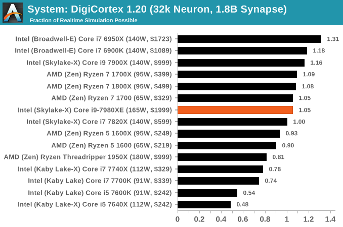
DigiCortex v1.20: link
Despite being a couple of years old, the DigiCortex software is a pet project for the visualization of neuron and synapse activity in the brain. The software comes with a variety of benchmark modes, and we take the small benchmark which runs a 32k neuron/1.8B synapse simulation. The results on the output are given as a fraction of whether the system can simulate in real-time, so anything above a value of one is suitable for real-time work. The benchmark offers a 'no firing synapse' mode, which in essence detects DRAM and bus speed, however we take the firing mode which adds CPU work with every firing.
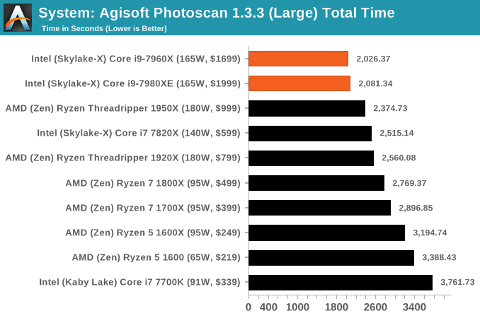
Agisoft Photoscan 1.3.3: link
Photoscan stays in our benchmark suite from the previous version, however now we are running on Windows 10 so features such as Speed Shift on the latest processors come into play. The concept of Photoscan is translating many 2D images into a 3D model - so the more detailed the images, and the more you have, the better the model. The algorithm has four stages, some single threaded and some multi-threaded, along with some cache/memory dependency in there as well. For some of the more variable threaded workload, features such as Speed Shift and XFR will be able to take advantage of CPU stalls or downtime, giving sizeable speedups on newer microarchitectures.
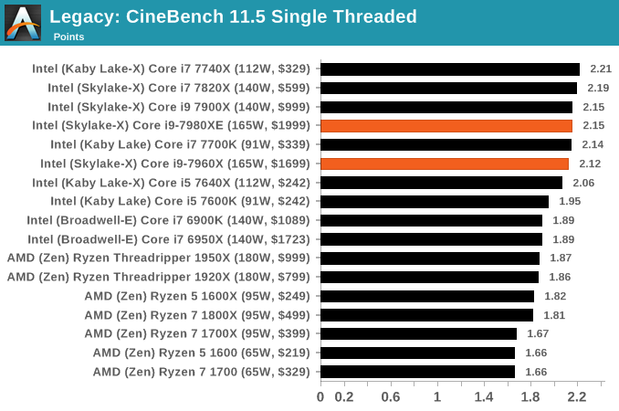
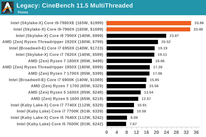
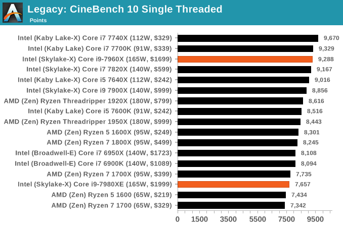
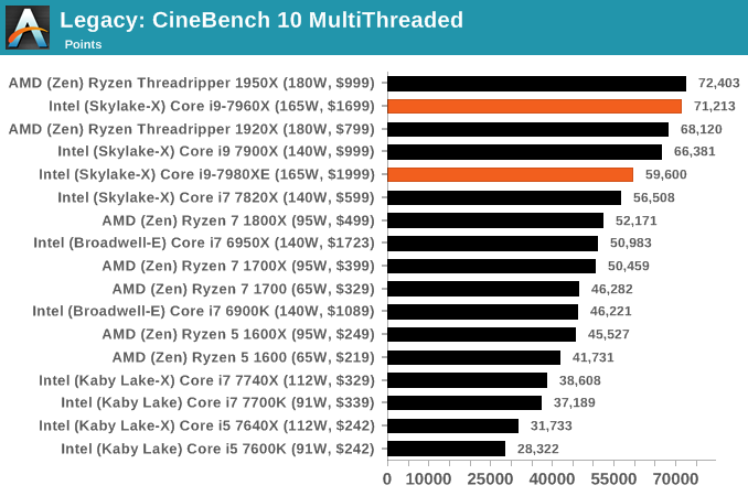
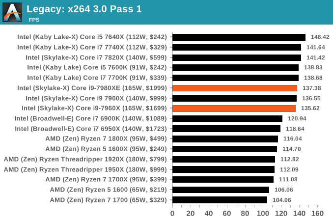
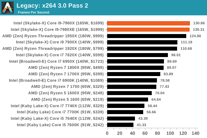
Benchmarking Performance: CPU Legacy Tests
Our legacy tests represent benchmarks that were once at the height of their time. Some of these are industry standard synthetics, and we have data going back over 10 years. All of the data here has been rerun on Windows 10, and we plan to go back several generations of components to see how performance has evolved.
All of our benchmark results can also be found in our benchmark engine, Bench.
3D Particle Movement v1
3DPM is a self-penned benchmark, taking basic 3D movement algorithms used in Brownian Motion simulations and testing them for speed. High floating point performance, MHz and IPC wins in the single thread version, whereas the multithread version has to handle the threads and loves more cores. This is the original version, written in the style of a typical non-computer science student coding up an algorithm for their theoretical problem, and comes without any non-obvious optimizations not already performed by the compiler, such as false sharing.
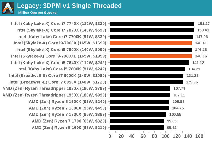

CineBench 11.5 and 10
Cinebench is a widely known benchmarking tool for measuring performance relative to MAXON's animation software Cinema 4D. Cinebench has been optimized over a decade and focuses on purely CPU horsepower, meaning if there is a discrepancy in pure throughput characteristics, Cinebench is likely to show that discrepancy. Arguably other software doesn't make use of all the tools available, so the real world relevance might purely be academic, but given our large database of data for Cinebench it seems difficult to ignore a small five minute test. We run the modern version 15 in this test, as well as the older 11.5 and 10 due to our back data.
x264 HD 3.0
Similarly, the x264 HD 3.0 package we use here is also kept for historic regressional data. The latest version is 5.0.1, and encodes a 1080p video clip into a high quality x264 file. Version 3.0 only performs the same test on a 720p file, and in most circumstances the software performance hits its limit on high end processors, but still works well for mainstream and low-end. Also, this version only takes a few minutes, whereas the latest can take over 90 minutes to run.
A Few Words on Power Consumption
When we tested the first wave of Skylake-X processors, one of the take away points was that Intel was starting to push the blurred line between thermal design power (TDP) and power consumption. Technically the TDP is a value, in Watts, to which a CPU cooler should be designed to cope with heat energy of that amount: a processor with a 140W TDP should be paired with a CPU cooler that can dissipate a minimum of 140W in order to avoid temperature spikes and ‘thermal runaway’. Failure to do so will cause the processor to hit thermal limits and reduce performance to compensate. Normally the TDP is, on average, also a good metric for power consumption values. A processor with a TDP of 140W should, in general, consume 140W of power (plus some efficiency losses).
In the past, particularly with mainstream processors, and even with the latest batch of mainstream processors, Intel typically rides the power consumption well under the rated TDP value. The Core i5-7600K for example has a TDP of 95W, and we measured a power consumption of ~61W, of which ~53W was from the CPU cores. So when we say that in the past Intel has been conservative with the TDP value, this is typically the sort of metric we will quote.
With the initial Skylake-X launch, things were a little different. Due to the high all-core frequencies, the new mesh topology, the advent of AVX-512, and the sheer number of cores in play, the power consumption was matching the TDP and even exceeding it in some cases. The Core i9-7900X is rated at 140W TDP, however we measured 149W, a 6.4% difference. The previous generation 10-core, the Core i7-6950X was also rated at 140W, but only draws 111W at load. Intel’s power strategy has changed with Skylake-X, particularly as we ramp up the number of cores.
Even though we didn’t perform the testing ourselves, our colleagues over at Tom’s Hardware, Paul Alcorn and Igor Wallossek, did extensive power testing on the Skylake-X processors. Along with showing that the power delivery system of the new motherboards works best with substantial heatsinks and active cooling (such as a VRM fan), they showed that with the right overclock, a user can draw over 330W without too much fuss.
So for the two processors in the review today, the same high values ring true. Almost to the point of it being alarmingly so. Both the Core i9-7980XE and the Core i9-7960X have a TDP rating of 165W, and we start with the peak headline numbers first. Our power testing implements a Prime95 stress test, with the data taken from the internal power management registers that the hardware uses to manage power delivery and frequency response. This method is not as accurate as a physical measurement, but is more universal, it removes the need to tool up every single product, and the hardware itself uses these values to make decisions about the performance response.
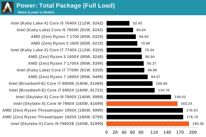
At full load, the total package power consumption for the Core i9-7960X is almost on the money, drawing 163W.
However the Core i9-7980XE goes above and beyond (and not necessarily in a good way). At full load, running an all-core frequency of 3.4 GHz, we recorded a total package power consumption of 190.36W. This is a 25W increase over the TDP value, or a 15.4% gain. Assuming our singular CPU is ‘representative’, I’d hazard a guess and say that the TDP value of this processor should be nearer 190W, or 205W to be on the safe side. Unfortunately, when Intel started designing the Basin Falls platform, it only was designed to be rated at 165W. This is a case of Intel pushing the margins, perhaps a little too far for some. It will be interesting to get the Xeon-W processors in for equivalent testing.
Our power testing program can also pull out a breakdown of the power consumption, depending if the registers are preconfigured in the software. In this case we were also able to pull out values for the DRAM controller(s) power consumption, although looking at the values this is likely to include the uncore/mesh as well. For both CPUs at load, we see that this DRAM and mesh combination is drawing ~42W. If we remove this from the load power numbers, that leaves 121W for the 16-core chip (7.5W per core) and 140W for the 18-core chip (7.8W per core).
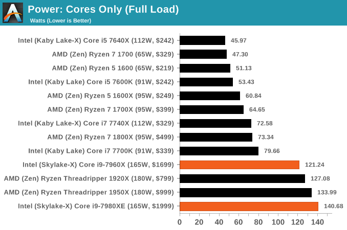
Most of the rise of the power consumption, for both the cores and DRAM, happens when the processor is loaded to four threads - the Core i9-7980XE is drawing 100W+ when four threads are loaded. This is what we expect to see: when the processor is lightly loaded and in turbo mode, a core can consume upwards of 20W, while at load it will migrate down to a smaller value. We saw the same with with Ryzen, drawing 17W per core when lightly threaded down to 6W per core when loaded. Obviously the peak efficiency point for these cores is down nearer the 6-8W range than up at the 15-20W range.
Unfortunately, due to timing, we did not perform any overclocking to see the effect it has on power. There was one number in the review materials we received that will likely be checked with our other Purch colleagues: one motherboard vendor quoted the power consumption of the Core i9-7980XE, when overclocked to 4.4 GHz, will reach over 500W. I think someone wants IBM’s record. It also means that the choice of CPU cooler is an important factor in all of this: very few off-the-shelf solutions will happily deal with 300W properly, let alone 500W. These processors are unlikely to bring about a boom in custom liquid cooling loops, however for the professionals that want all the cores and also peak single thread performance, start looking at pre-built overclocked systems that emphasize a massive amount of cooling capability.
A Quick Run on Efficiency
Some of our readers have requested a look into some efficiency numbers. We’re still in the process of producing a good way to represent this data, and take power numbers directly during the benchmark to get a full accurate reading. In the meantime, we’re going to take a benchmark we know hammers every thread of every CPU and put that against our load power readings.
First up is Corona. We take the benchmark result and divide by the load power, to get the efficiency value. This value is then reduced by a constant factor to provide a single digit number.
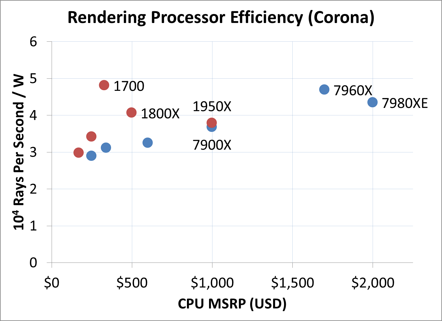
In a rendering task like Corona, where all the threads are hammered all the time, both the Skylake-X parts out-perform Threadripper for power efficiency, although not by twice as much. Interestingly the results show that as we reduce the clocks on TR, the 1700 comes out on top for pure efficiency in this test.
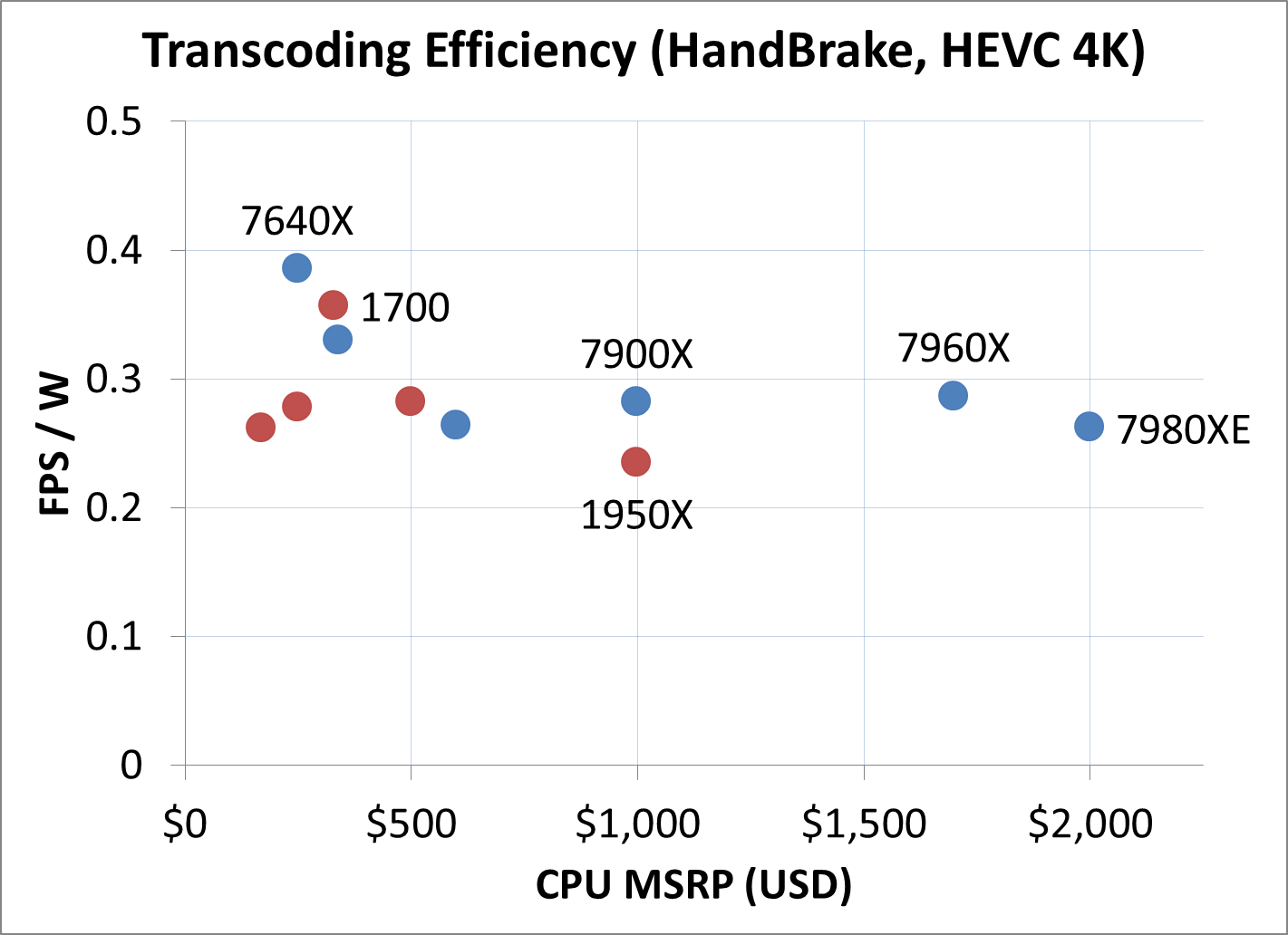
HandBrake’s HEVC efficiency with large frames actually peaks with the Core i5 here, with the 1700 not far behind. All the Skylake-X processors out-perform Threadripper on efficiency.
Analyzing Performance Per Dollar
While measuring the performance per watt is an interesting metric, workstation processors are at the top of the stack when it comes to power consumption: the point of these processors (typically) is getting work done fast, and their users don't mind using a bit more power to get there. When it comes to designing a workstation level system for an office, the person who signs off on the project is not going to look at the performance per watt - they are going to look at the performance per dollar. Does this purchase represent the best value for the environment, and is the purchase likely to give us the best return? The following graphs attempt to answer that information, and we've chosen a varied selection including variable threaded loads.
For this analysis, we've taken all of the processors we have tested from what Intel has launched in 2017. This covers all of the consumer level Kaby Lake-S i7 and i5 parts (except T), the high-end desktop Kaby Lake-X processors, and all the high-end Skylake-X desktop parts. This is represented in the graphs in blue under the 'Intel 2017' title. From AMD, we have all eleven AMD Ryzen processors tested, under the red line.
Compile Performance Per Dollar
One of our popular benchmarks is our compile test. This takes a fixed version of Chromium v56, and runs it through the MSVC compiler with linking as per the directions given on by the Chromium developers. A typical test can run from 40 minutes to 3 hours depending on the processor, and taxes the single thread, the multi-thread and the memory performance of the system. We've seen that it does not particularly take kindly to processors with victim caches, such as Skylake-X or AMD Ryzen, with limited scaling on the code workflow. Despite the per-core performance dip from Skylake-S to Skylake-X, the top processor still has the best absolute performance. Converting our data to the number of compiles per day per dollar gives the following graph:

The cheaper end of the graph is surprisingly high, dominated by Intel's dual-core Pentium (with hyperthreading) being offered for super low prices. In the standard 'consumer' price range below $300, the mid-range Ryzen processors have a slight advantage, but, beyond the Ryzen 7 1700, Intel has the performance per dollar advantage all the way out to $2000.
Agisoft Performance Per Dollar
The Agisoft Photoscan software has been a key part of our performance testing for several years, demonstrating a true office workflow: archival purposes of taking 2D photos and converting them into 3D models. This is a computationally interesting algorithm, involving multiple single-threaded and multi-threaded stages.
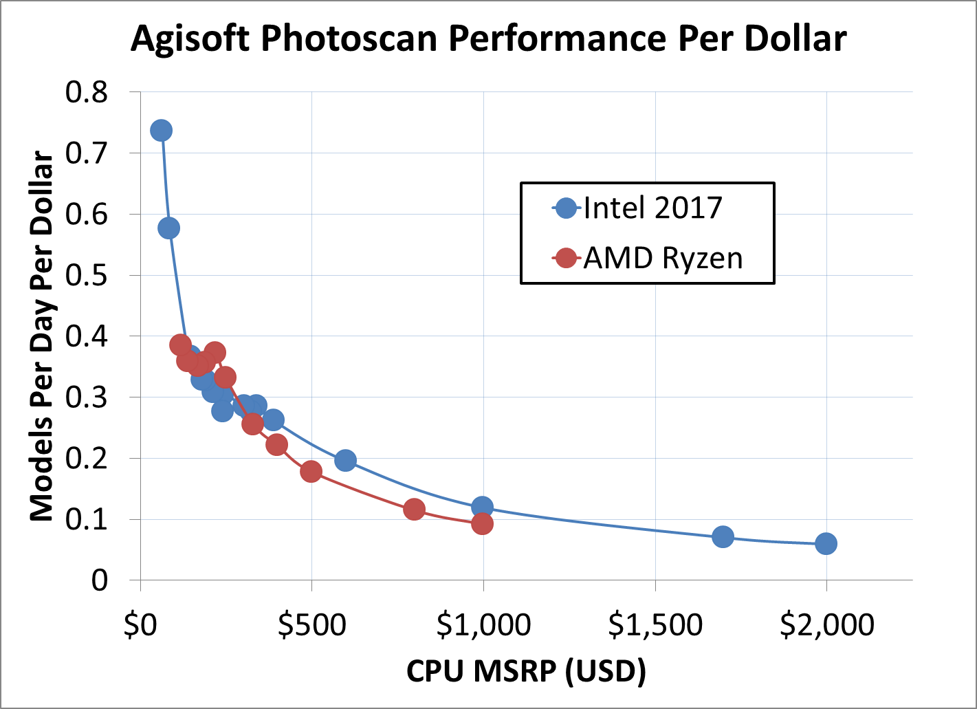
Due to the single threaded elements of the algorithm, linear scaling is not observed as we ramp up through the core counts. At the mid-range consumer processor pricing, the twelve-thread Ryzen 5 processors sit above the quad-thread Core i5 parts, but beyond $330 or so, as we move into Intel's quad-core offerings and above, the performance per dollar is solely on Intel's side.
Blender Performance Per Dollar
The Blender benchmark has been an interesting debate in the last few months, with the new architectures from Intel and AMD pushing updates into the code for faster rendering. Our test takes a well used Blender release and one of the standard benchmarks (rather than anything vendor specified). Results are given in renders of this benchmark per day per dollar.
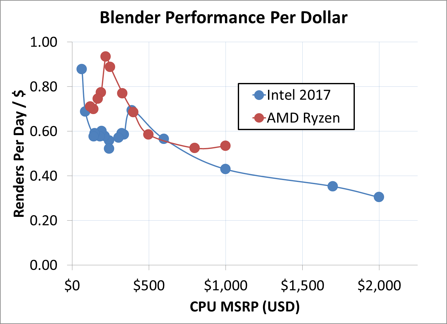
Interestingly AMD takes the peak PPD across the full range. At $999, where the competition is expected to be highest, AMD has over a 10% advantage. In the four digit range, even though the PPD of Intel's processors is lower, the absolute performance is still better. For our Blender test, this translates so a few seconds over a 2-3 minute test.
Cinebench R15 nT Performance Per Dollar
Next we move into the pure multithreaded benchmarks, which can be a significant number of workstation workloads. Here Intel might be at a disadvantage, with AMD offering more cores and more threads at each price point - Intel's IPC advantage will have to offset this in order to move ahead.
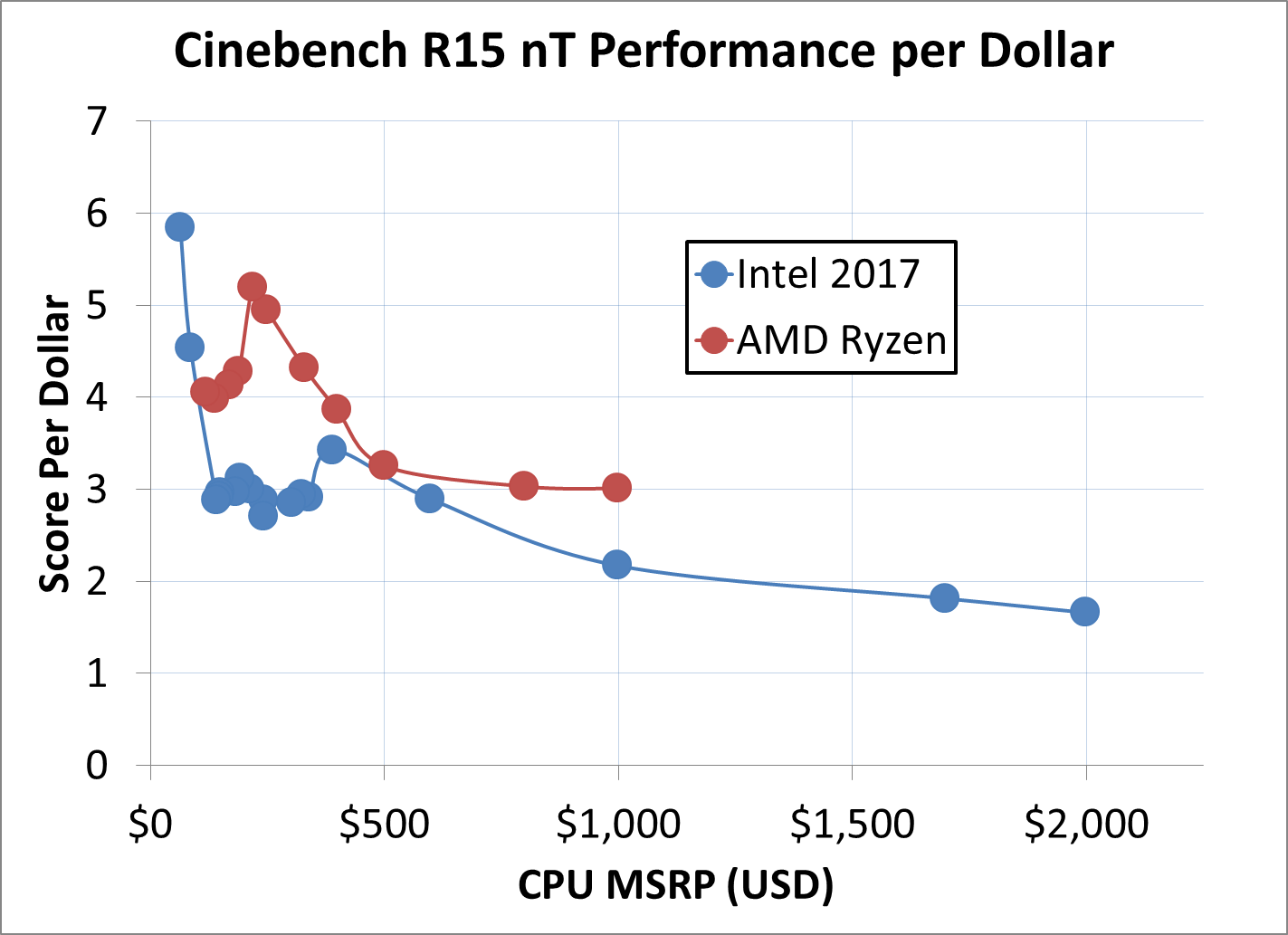
To lay some background here: AMD has been plugging Cinebench R15 nT benchmark numbers since the launch of Zen, citing better PPD. Intel's rebuttal is that in absolute performance, when you need the absolute best results, their hardware still wins.
Corona Rendering Performance Per Dollar
Ray tracing is another example of light threads taking advantage of more cores, more frequency, higher IPC and accelerated intructions with fast FP throughput. Citing back to Johan's EPYC review again, which showed AMD's good base FP performance, it will be an interesting comparison.
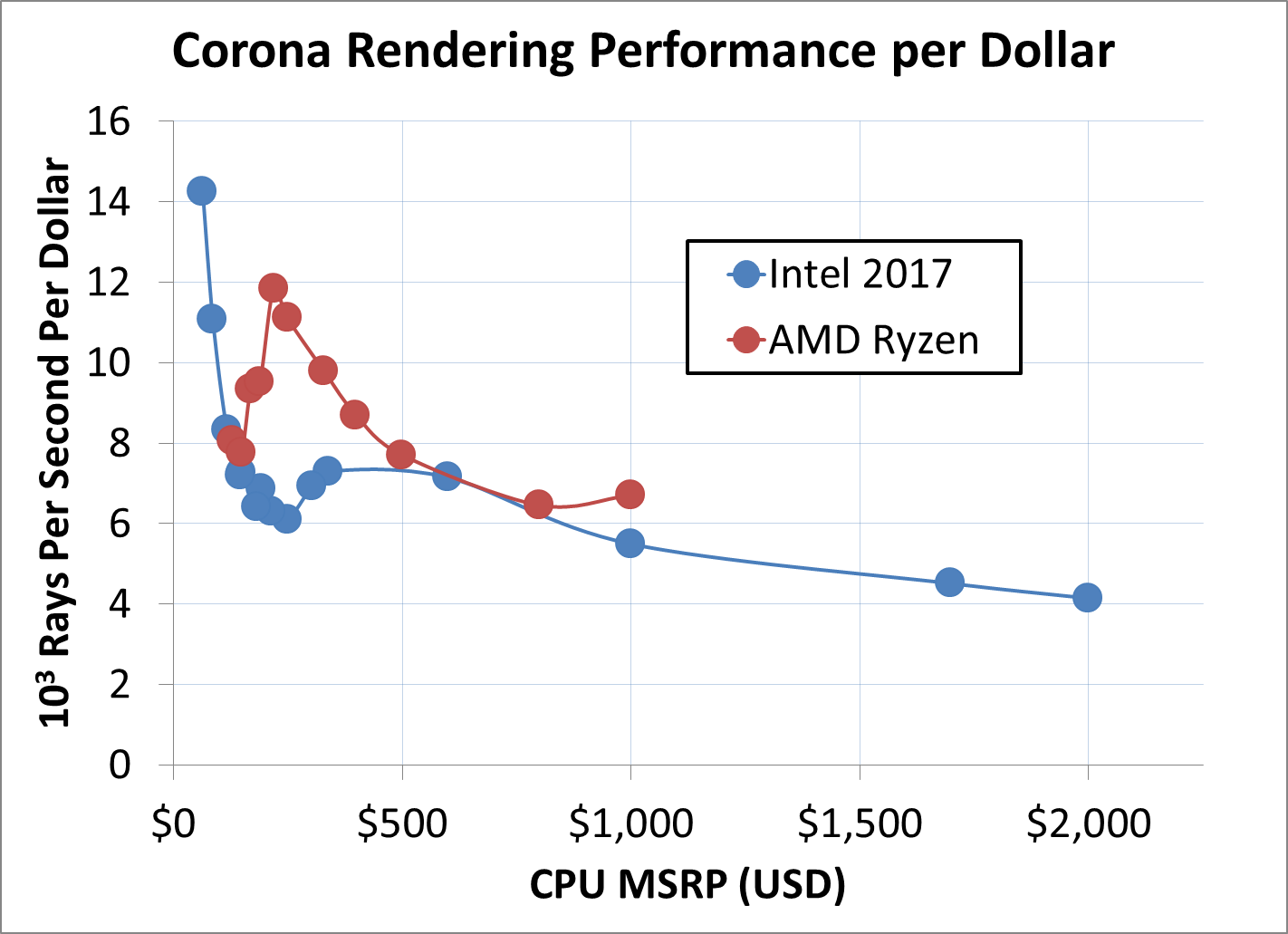
Similar to some of the previous graphs, the best PPD is held at Intel's low end Pentium processors - however these do not give the best overall throughput. In the mainstream price range, the Ryzen 5 1600 and 1600X are suprising peak results. In the $500-$800 range, Intel and AMD are about equal, however at $999 the Threadripper is ahead of the Core i9. Again, at the $1500+ range, Intel offers the better overall throughput, despite the lower PPD.
Intel Core i9-7980XE and Core i9-7960X Conclusion
In the 2000s, we had the frequency wars. Trying to pump all the MHz into a single core ended up mega-hurting one company in particular, until the push was made to multi-core and efficient systems. Now in the 2010s, we have the Core Wars. You need to have at least 16 cores to play, and be prepared to burn power like never before. With today’s launch, Intel has kicked their high-end desktop offerings up a notch, both in performance and power consumption.
Pun density aside, both Intel and AMD are pursuing a many-core strategy when it comes to the high-end desktop. Both manufacturers have the same story in their pockets: users need more multi-threaded performance, either for intense compute or for a heavy scoop of compute-based multi-tasking, to include streaming, encoding, rendering, and high-intensity minesweeper VR all at the same time. Due to having so many cores, single threaded performance while under load can be lower than usual, so both companies focus on throughput rather than responsiveness.
The Core i9-7980XE is Intel’s new top-of-the-line HEDT processor. Coming in at 18-cores and drawing 165W, this processor can reach 4.4 GHz at top turbo or 3.4 GHz on all-core turbo. At $1999, it becomes the most expensive (?) consumer focused processor on the market. It is priced at this level for two reasons: first such that it doesn’t cannibalize Intel’s enterprise sales which have a higher profit margin, but also due to Intel’s product stack it fills up several price points from $300 all the way to $2000 now, and with it being Intel’s best consumer processor, they are hoping that it will still sell like hot cakes.
Our performance numbers show that Intel’s best multi-core consumer processor is deserving of that title. In most of our multi-core tests, Intel has a clear lead over AMD: a combination of more cores and a higher single threaded performance compensates for any frequency difference. For anyone with hardcore compute, Intel gets you to the finishing line first in almost every scenario. AMD does win on a few benchmarks, which is something we saw when Johan tested the enterprise versions of Intel's and AMD's CPUs in his review, where he cited AMD’s FP unit as being the leading cause of the performance improvement.
There are going to be three cautionary flags to this tale based on our testing today, for anyone looking at Skylake-X, and they all start with the letter P: Power, Platform, and Price.
Power: In our testing, Intel’s cores can consume between 20W and 7.5W per core, which is a large range. When all cores are at load, as well as the mesh and DRAM controllers, the Core i9-7980XE draws over 190W, well above the TDP rating of 165W. This will cause concern for users that take the TDP value as rote for power consumption – and for any users thinking of overclocking it might also be worth investing in custom cooling loops. The processors from AMD consume ~177W at load, which for two cores less is about the same ballpark.
Platform: X299 motherboards are designed to handle Kaby Lake-X, Skylake-X LCC and Skylake-X HCC processors. Almost all the motherboards should be geared towards the high-end processors which makes platform compatibility a bit of a non-issue, however testing by others recommends some form of active cooling on the power delivery. When investing $1999 in a processor, especially if a user is considering overclocking, it is likely that a good motherboard is needed, and not just the bargain basement model. Some users will point to the competition, where AMD's processors offer enough lanes for three x16 GPUs and three PCIe 3.0 x4 storage devices from the processor at the same time, rather than reduced bandwidth for 3-way and requiring storage to go through the chipset.
Price: $1999 is a new record for consumer processors. Intel is charging this much because it can – this processor does take the absolute workstation performance crown. For high performance, that is usually enough – the sort of users that are interested in this level of performance are not overly interested in performance per dollar, especially if a software license is nearer $10k. However for everyone else, unless you can take advantage of TSX or AVX-512, the price is exorbitant, and all arrows point towards AMD instead. Half the price is hard to ignore.
Users looking at the new processors for workstation use should consider the three Ps. It’s not an easy task, and will highly depend on the user specific workflow. The recommendations ultimately come down to three suggestions:
- If a user needs the top best workstation processor without ECC, then get Skylake-X.
- If a user needs ECC or 512GB of DRAM, Xeon-W looks a better bet.
- If a user has a strict budget or wants another GPU for compute workloads, look at Threadripper.
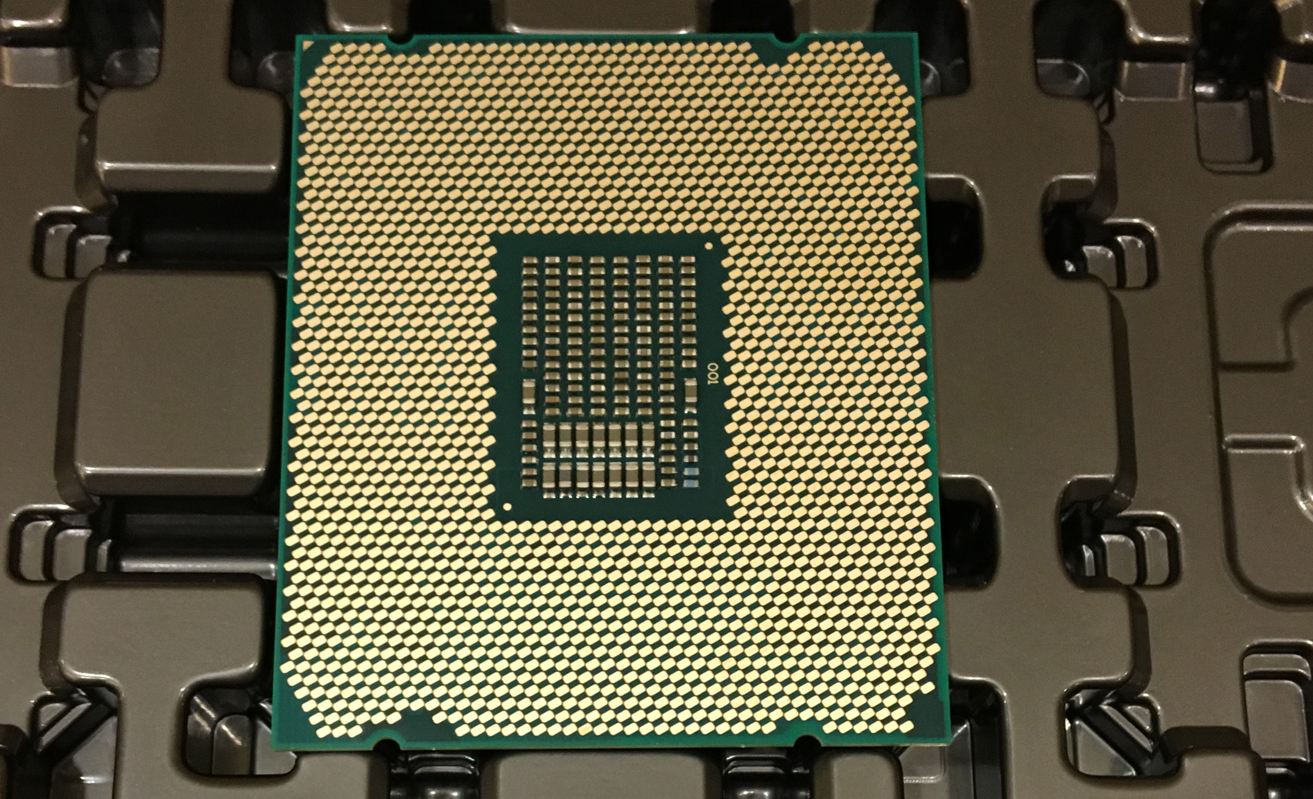
For those weighing up the Core i9-7960X compared to the Core i9-7980XE, part of me wants to say ‘if you’re going for cores and prepared to spend this much, then go all the way’. If the main purpose is throughput, for the benchmarks that matter, the 7980XE is likely to provide benefit. For multi-taskers, the benefits are less clear, and it would be interesting to get the Core i9-7940X and Core i9-7920X in for testing.


