Original Link: https://www.anandtech.com/show/12834/arm-announces-the-mali-g76-scaling-up-bifrost
Arm Announces Mali-G76 GPU: Scaling up Bifrost
by Ryan Smith & Andrei Frumusanu on May 31, 2018 3:00 PM EST
Section by Andrei Frumusanu
It’s been two years since Arm announced their first “next-generation” GPU architecture based on Bifrost and alongside with it its first implementation the G71. Following its release in the first products the GPU was off to a very shaky start as the G71 was quite a disaster in the Kirin 960 and Exynos 8895 as both GPU implementations blew past their power budgets in severe manners.
This year’s G72 was a much more reasonable product as it offered up to a 100% improvement in efficiency in the Kirin 970 and Exynos 9810, putting the G72 a lot nearer to the performance and efficiency targets that the Bifrost architecture was promised to achieve.
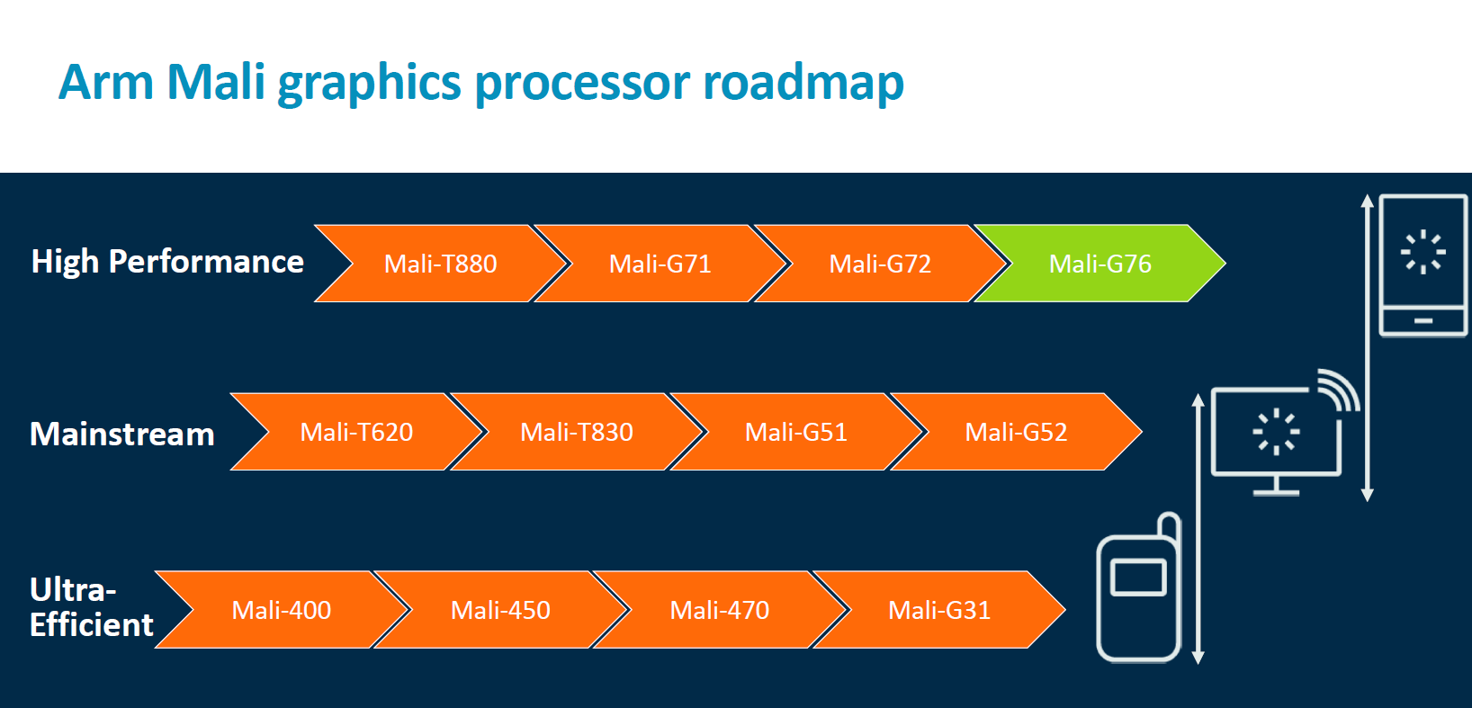
Today’s Arm announces the follow-up to the G72 and the latest offspring in the Bifrost family: The Mali G76. The targets of the GPU IP should be pretty clear: Improve performance, efficiency and area and try to catch up with the competition as much as possible.
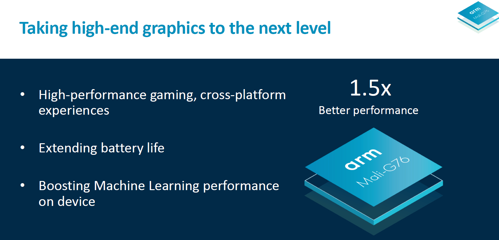
Overall what Arm promises for the next generation of SoCs using the G76 on a new TSMC 7nm process is a 50% increase in performance versus current generation devices.
In terms of apples-to-apples comparisons, we see three key metrics that are improved: A 30% improvement in performance density is the first one. What this means is that either for the same area, the new GPU will perform 30% better, or for the same performance, the vendor can shrink the GPU space on the SoC.
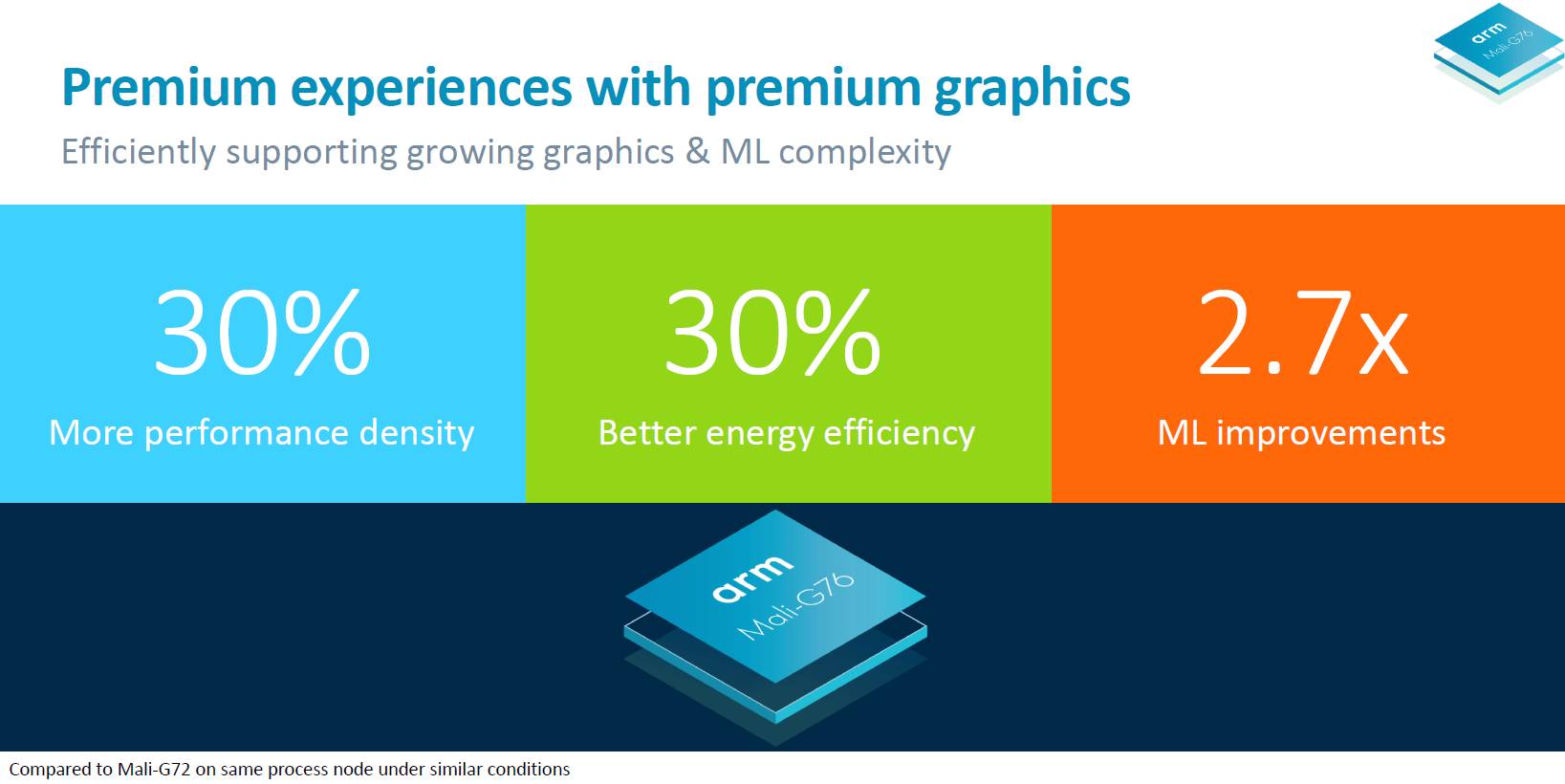
The new GPU promises a 30% microarchitectural efficiency improvement thanks to a consolidation of the functional blocks of the unit. Efficiency is particularly something Arm needs to focus on in regards to Mali as we’ve seen a few missteps over the last year or two and the competition from Qualcomm in the GPU and 3D gaming space is particularly fierce.
Finally, there’s a quoted 2.7x improvement for machine learning inferencing applications thanks to the inclusion of new dedicated 8-bit dot product instructions.
The Mali G76 - Scaling It Up
Section by Ryan Smith
Mali-G76 is an interesting change for Arm’s GPU designs, both because it changes some fundamental aspects of the Bifrost architecture, and yet it doesn’t.
At a very high level, there are no feature changes with respect to graphics, and only some small changes when it comes to compute (more on that in a moment). So there is little to talk about with regards here in terms of end-user functionality or flashy features. Bifrost was already a modern graphics architecture, and the state of 3D graphics technology hasn’t significantly changed in the last two years to invalidate that.
Instead, like Mali-G72 before it, G76 is another optimization pass on the underpinnings of the architecture. And compared to G72, G76 is a much greater pass that as a result makes some significant changes in how Arm’s GPUs work. It’s still very much the Bifrost architecture, but it’s actually one of the biggest changes we’ve ever seen within a single graphics architecture from one revision to the next, and that goes for both mobile and PC.
The big change here is that in an effort to further boost the performance and area efficiency of the architecture, Arm is doubling the width of their fundamental compute block, the “quad” execution engine. In both the Mali-G71 and G72, a quad is just that: a 4-wide SIMD unit, with each lane possessing separate FMA and ADD/SF pipes. Fittingly, the width of a wavefront at the ISA-level for these parts has also been just 4 instructions, meaning all of the threads within a wavefront are issued in a single cycle. Overall, Bifrost’s use of a 4-wide design was a notably narrow choice relative to most other graphics architectures.
But the quad is a quad no longer. For Mali-G76, Arm is going big. The eponymous quad is now an 8-wide SIMD. In other words, a Mali-G76 quad – and for that matter an entire core – now has twice as many ALUs as before. All of the features are the same, as is the execution model within a quad, but now Arm can weave together and execute 8 threads per clock per quad versus 4 on past Bifrost parts.
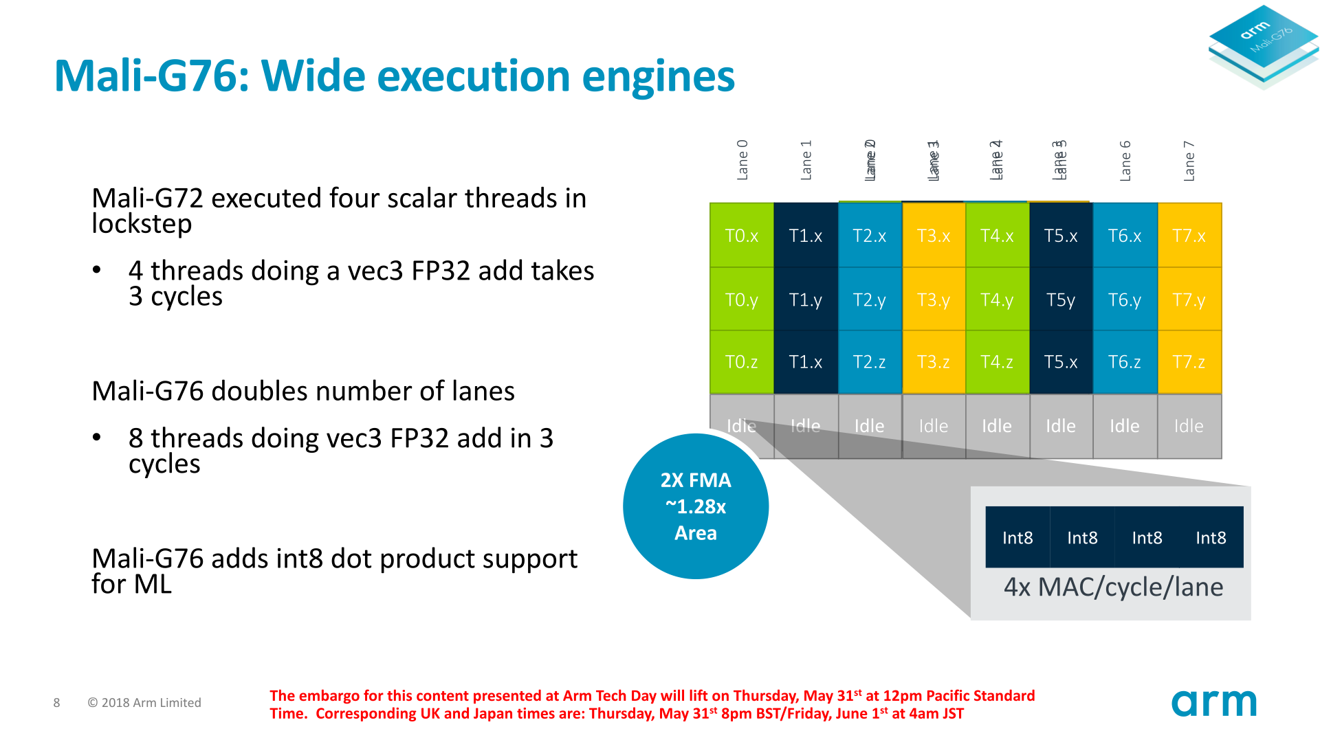
This is a very interesting change because, simply put, the size of a wavefront is typically a defining feature of an architecture. For long-lived architectures, especially in the PC space, wavefront sizes haven’t changed for years. NVIDIA has used a 32-wide wavefront(warp) going all the way back in G80 in 2006, and AMD’s 64-wide wavefront goes back to the pre-GCN days. As a result this is the first time we have seen a vendor change the size of their wavefron in the middle of an architectural generation.
Now there are several ramifications of this, both for efficiency purposes and coding purposes. But before going too far, I want to quickly recap part of our Mali-G71 article from 2016, discussing the rationale for Arm’s original 4-wide wavefront design.
Moving on, within the Bifrost architecture, ARM’s wavefronts are called Quads. True to the name, these are natively 4 threads wide, and a row of instructions from a full quad is executed per clock cycle. Bifrost’s wavefront size is particularly interesting here, as quads are much smaller than competing architectures, which are typically in the 16-32 thread range. Wavefront design in general reflects the need to find a balance between resource/area density and performance. Wide wavefronts require less control logic (ex: 32 threads with 1 unit of control logic, versus 4x8 threads with 8 units of control logic), but at the same time the wider the wavefront, the harder it is to fill.ARM’s GPU philosophy in general has been concerned with trying to avoid execution stalls, and their choice in wavefront size reflects this. By going with a narrower wavefront, a group of threads is less likely to diverge – that is, take different paths, typically as a result of a conditional statement – than a wider wavefront. Divergences are easy enough to handle (just follow both paths), but the split hurts performance.
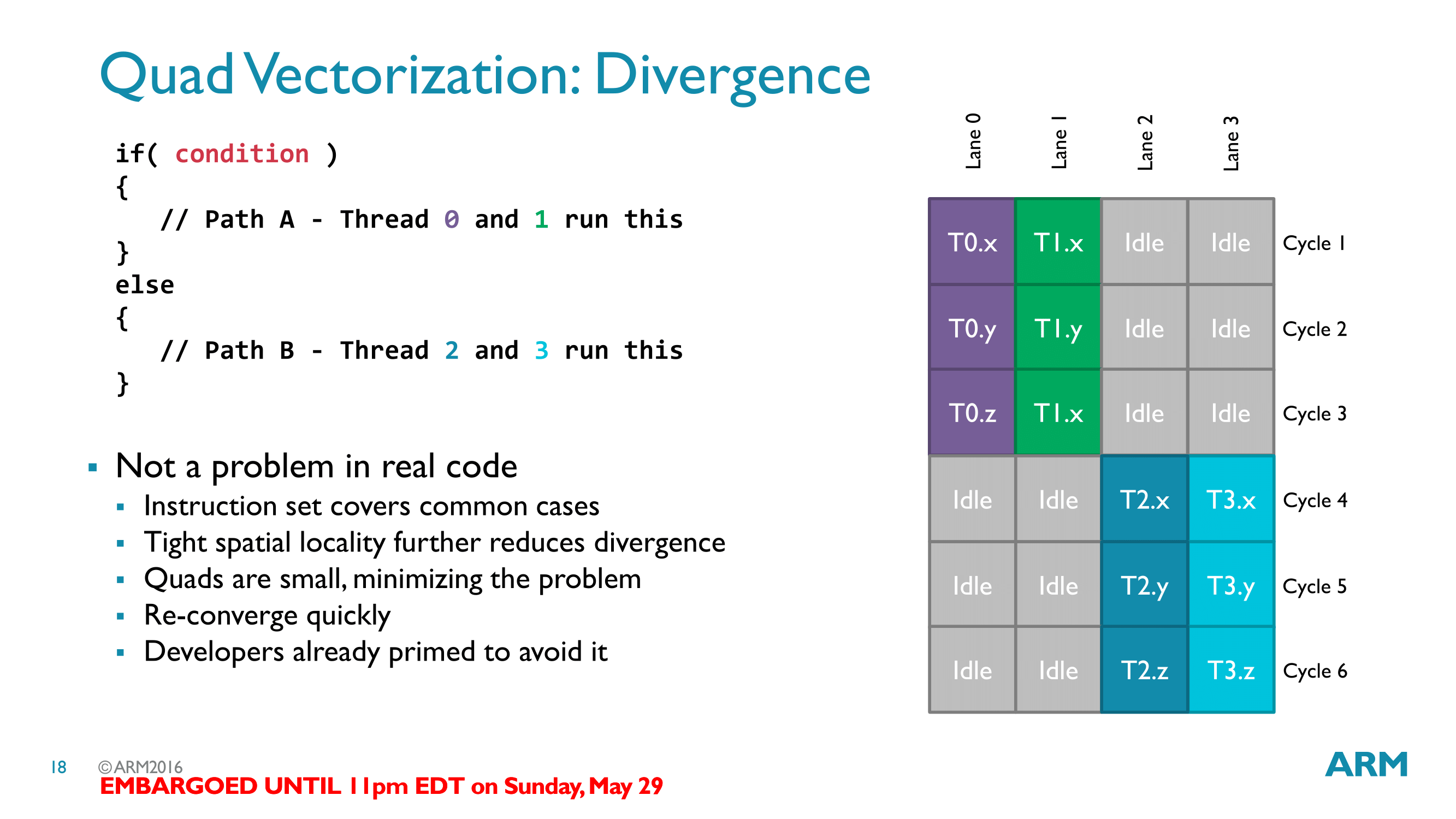
At the time, Arm said that they went with a 4-wide wavefront in order to minimize the occurrence of idle ALUs from thread divergence. On paper this is a sound strategy, as if you’re expecting a lot of branching code, then those ALUs are doing nothing of value for you if they’re idle due to thread divergence. A great deal of effort goes into balancing an architecture design around this choice, and particularly in the PC space, once you choose a size you’re essentially stuck with it as developers will optimize against this.
However the trade-off for a narrow wavefront and the resulting SIMDs is that the ratio of control logic to ALUs is quite a bit higher. Every SIMD is supported by a mix of cache, dispatch control hardware, internal datapaths, and other hardware. The size of this logic is somewhat fixed due to its functionality, so a wider SIMD doesn’t require much of an increase in the size of the supporting hardware. And it’s this trade-off that Arm is targeting for Mali-G76.
The net result of switching to an 8-wide SIMD design here is that Arm is decreasing the control logic to ALU ratio – or perhaps it’s better said that they’re increasing the ratio of ALUs to control logic. In the case of G76, for example, despite doubling the lanes and theoretical throughput of an execution engine, the resulting block is only about 28% larger than one of Mali-G72’s engines. Scale this up over an entire GPU, and you can easily see how this can be a more area-efficient option.

Though not explicitly said by Arm in their briefings, our interpretation of this change is that it’s a bit of an admittance that the 4-wide design of the original Bifrost architecture was overzealous; that thread divergence in real-world code isn’t high enough to justify the need for such a narrow SIMD. For their part, Arm did confirm that they see the granularity requirements of GPU code (games and compute alike) being different than what they were when G71 launched. And in the meantime this also helps Arm’s scalability efforts, as the more area-dense quad design means that Arm can pack more of them in the same die space, getting a larger number of ALUs per mm2 overall.
This change also brings the Mali-G7x GPUs in-line with the Mali-G52, which uses the same 8-wide SIMD design and was launched by Arm in a more low-key manner back in March of this year. So while G76 is technically the second Arm GPU design announced with this change, it’s been our first real chance to sit down with Arm and see what they’re thinking.
It goes without saying then that we’re curious to see what the real-world performance impacts of this change are like. Given just how uncommonly narrow Arm’s quads were, it should be pretty easy to similarly fill an 8-wide SIMD design, and in that respect, I suspect Arm is right about wider being a better choice. However wider designs do require some smarter compiler programming in order to ensure you can keep the wider SIMDs similarly filled, so Arm’s driver team has a part to play in all of this as well.
Thankfully for Arm, the mobile market is not nearly as bound to wavefront size as the PC market is, which allows for Arm to get away with a mid-generation change like this. Developers aren’t writing customized code specifically for Arm’s GPUs in the way they are in the PC space, rather everything is significantly abstracted (and overall left rather generic) through OpenGL ES, Vulkan, and other graphics/compute APIs. So for mobile developers and for existing game/application binaries, this underlying change should be completely hidden by the combination of APIs and Arm’s drivers.
As an aside, doubling the number of SIMD lanes within a quad has also led Arm to double the relevant supporting cache and pathways as well. While Arm doesn’t officially disclose the size of a quad’s register file, they have confirmed that there are 64 registers per lane for G76’s register file, just like there was for Mali-G72. So on a relative basis, register file pressure is unchanged.

Fittingly, Arm has also doubled the throughput of their pixel and texel hardware to keep up with the wider quads. A single core can now spit out 2 texels and 2 pixels per clock, maintaining the same ALU/texture and ALU/pixel ratios as before. To signify this on the Mali-G76, Arm now calls this their “Dual Texture Unit”, as opposed to the single “Texture Unit” on G72 and G71.

The end result of all of this, as Andrei once put it, is that in a sense Arm has smashed together two Mali-G72 cores together to make a single G76 core. At equal clockspeeds compute, texture, and pixel throughput have all been doubled, and on paper will result in virtually identical performance. However the benefit to Arm is that this design takes up a lot less space than two whole cores; Arm essentially gets the same per-clock performance in about 66% of the die area of an equivalent G72 design, greatly boosting their area efficiency, an always important metric for the silicon integrators who bring Arm’s GPU designs to life.
The Mali G76 µarch - Fine Tuning It
Section by Ryan Smith
While the biggest change in the G72 is by far Arm’s vastly wider cores, it’s not the only change to come to the Bifrost architecture. The company has also undertaken a few smaller changes to further optimize the architecture and improve performance efficiency.
First off, within their ALUs Arm has added support for Int8 dot products. These operations are becoming increasingly important in machine learning inference, as it’s a critical operation in processing neural networks and despite the limited precision, is still deep enough for basic inference in a number of cases. To be sure, even the original Bifrost already natively supported Int8 data types, including packing 4 of them into a single lane, but G76 becomes the first to be able to use them in a dot product in a single cycle.
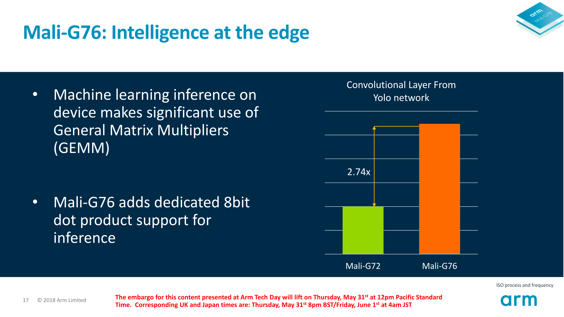
As a result, Arm is touting a 2.7x increase in machine learning performance. This will of course depend on the workload – particularly the framework and model used – so it’s just a high-level approximation. But Arm is betting big on machine learning, so significantly speeding up GPU machine learning inference gives Arm’s customers another option for efficiently processing these neural networks.
Meanwhile, in part as a consequence of the better scalability of Mali-G76’s core design, Arm has also taken a look at other aspects of GPU scalability to improve performance. Their research found that another potential scaling bottleneck is the tiler, which could block the rest of the GPU if it stalled during a polygon writeback. As a result, Arm has moved from an in-order writeback mechanism to an out-of-order writeback mechanism, allowing for polygons to be written back with more flexibility by bypassing those writeback stalls. Unfortunately Arm is being somewhat mum here on how this was implemented – generally changing an in-order process to out-of-order is not a simple task – so we haven’t been given much other information on the matter.
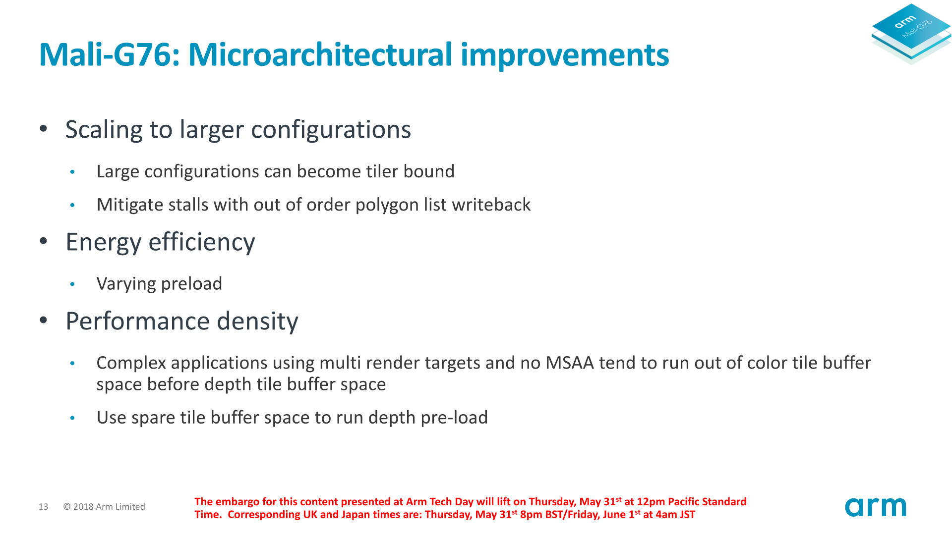
Arm has also made a subtle but important change to how their tile buffers can be used in an effort to keep more traffic local to the GPU core. In certain cases, it’s now possible for applications that run out of color tile buffer space to spill over into the depth tile buffer. Arm is specifically citing workloads involving heavy use of multiple render targets without MSAA for driving this change; the lack of MSAA means that the depth tile buffer is used only sparingly, while the multiple render targets quickly chew through the color tile buffer rather quickly. The net result of this is that it cuts down on the number of trips that need to be made to main memory, which is a rather expensive operation.

Speaking of spilling, G76’s thread local storage mechanism has also been optimized for how it handles register spills. Now the GPU will attempt to group data chunks from spills together so that they can be more easily fetched in the future. This is as opposed to how earlier GPUs did it, where register spills were scattered based on which SIMD lane the data ultimately belonged to.
Section by Andrei Frumusanu
Performance & Efficiency
In terms of scalability and performance, what we can generally say is that one G76 core is roughly equal to two G72 cores. This also changes the configuration options that Arm offers as the maximum core count for the largest GPU is an MP20 configuration.
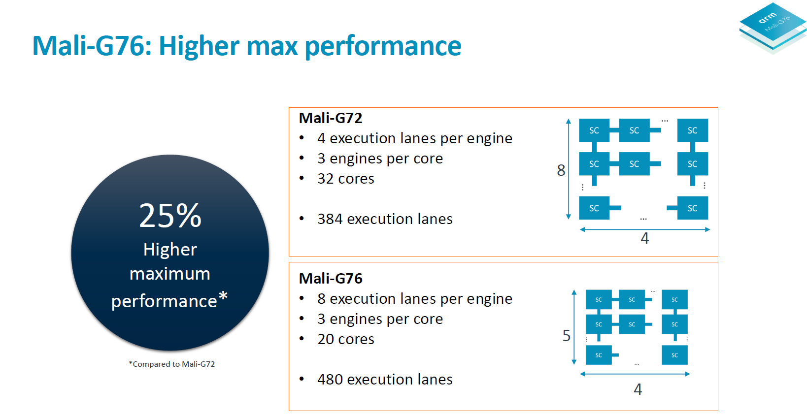
When going all-out in laying down cores this means we have a 25% higher maximum performance point. To date we haven’t seen vendors reach near the maximum configuration option of MP32 for the G71 and G72 and as the largest Mali was the Exynos 8895 with a G71MP20.
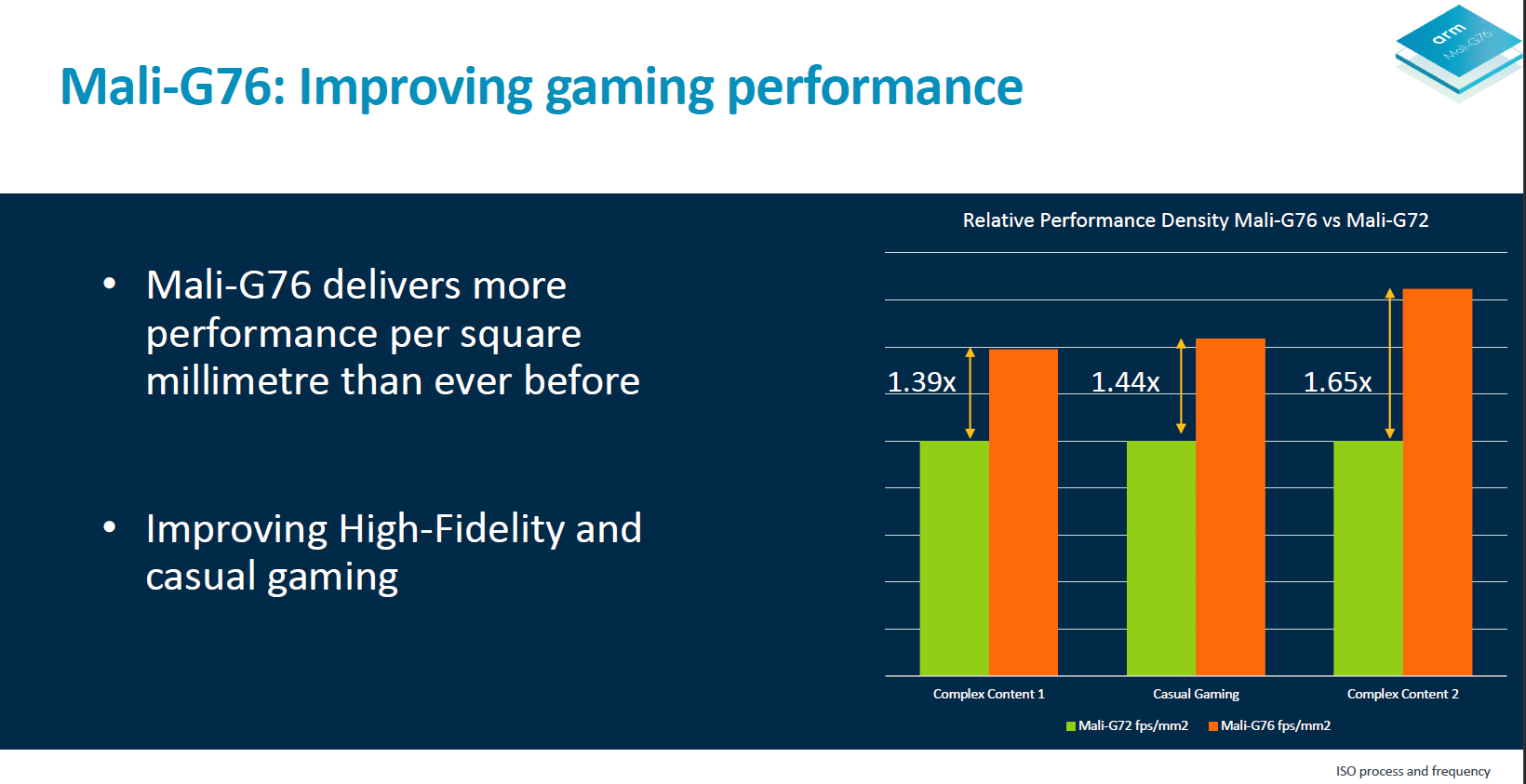
Improving the performance density of the cores by consolidating functional blocks and execution engines in fewer “cores” improves the PPA of the GPU dramatically. The G76 at iso process and frequency, at similar area configurations, is said to improve the fps/mm² metric by 39% in Manhattan 3.0 and thanks to the improvements in the geometry pipelines, a significant 65% in Car Chase. The casual gaming benchmark here depicts a simpler fill-rate bound workload such as Angry Birds and Candy Crush.
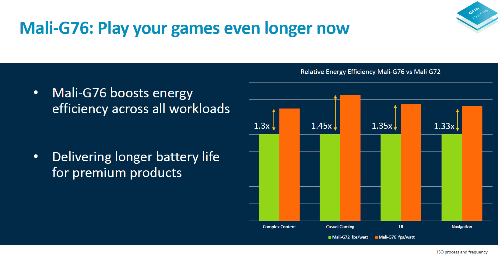
In terms of power efficiency, the metrics presented here depict the performance improvement at ISO process node and frequency, at ISO power values of peak power coming in at a target 2.3W GPU power only. We’re to be reminded that for 3D workloads there’s significant power overhead from the memory subsystem and DRAM and that’s why this figure is lower than what I’ve usually published in terms of total platform active power in the past.
In general the figures that we’re looking at in terms of improvement in common benchmarks like Manhattan are a 1.3x increase in performance at equal power and area, process and frequency.
How this would look in a late 2018 / early 2019 SoC would be something like the following projection:
| GFXBench Manhattan 3.1 Offscreen Power Efficiency (System Active Power) |
||||
| Mfc. Process | FPS | Avg. Power (W) |
Perf/W Efficiency |
|
| Mali G76MP12 SoC Projection | 7/8nm class | 69.00 | 4.08 | 16.90 fps/W |
| Galaxy S9+ (Snapdragon 845) | 10LPP | 61.16 | 5.01 | 11.99 fps/W |
| Galaxy S9 (Exynos 9810) | 10LPP | 46.04 | 4.08 | 11.28 fps/W |
| Galaxy S8 (Snapdragon 835) | 10LPE | 38.90 | 3.79 | 10.26 fps/W |
| LeEco Le Pro3 (Snapdragon 821) | 14LPP | 33.04 | 4.18 | 7.90 fps/W |
| Galaxy S7 (Snapdragon 820) | 14LPP | 30.98 | 3.98 | 7.78 fps/W |
| Huawei Mate 10 (Kirin 970) | 10FF | 37.66 | 6.33 | 5.94 fps/W |
| Galaxy S8 (Exynos 8895) | 10LPE | 42.49 | 7.35 | 5.78 fps/W |
| Galaxy S7 (Exynos 8890) | 14LPP | 29.41 | 5.95 | 4.94 fps/W |
| Meizu PRO 5 (Exynos 7420) | 14LPE | 14.45 | 3.47 | 4.16 fps/W |
| Nexus 6P (Snapdragon 810 v2.1) | 20Soc | 21.94 | 5.44 | 4.03 fps/W |
| Huawei Mate 8 (Kirin 950) | 16FF+ | 10.37 | 2.75 | 3.77 fps/W |
| Huawei Mate 9 (Kirin 960) | 16FFC | 32.49 | 8.63 | 3.77 fps/W |
| Huawei P9 (Kirin 955) | 16FF+ | 10.59 | 2.98 | 3.55 fps/W |
Arm that’s that the 1.5x target improvement in performance on a future G76 in 7nm would happen thanks to a relative increase of the GPU capabilities scaling from a G72MP18 to a G76MP12. So it seem natural to take the Exynos 9810 as a baseline for the performance projections. Assuming the power target wouldn’t change, we’d see a G76MP12 in the upcoming process node outperforming current generation leader, the Snapdragon 845, by 13% in Manhattan 3.1. Power efficiency at peak performance would also be 47% better.
Obviously the competition won’t be standing still – although Qualcomm had a bit of a misstep in terms of power efficiency in the Adreno 630, it’s possible this will be caught up in the next iteration next year, not to mention that the process node improvements alone would be then sufficient to retake the lead on the GPU side.
End Remarks
All in all, the Mali G76 provides extremely solid advancements – 30% better performance at the same area and power are heavy generational improvements. However while this will greatly improve the competitiveness of Mali GPUs – I don’t think it will be quite sufficient to catch up with the competition.
In terms of the microarchitectural changes, I think Arm did the right choices in terms of consolidating the cores and beefing them up. Currently it seems that the high-core count in Mali GPUs is a two-edged sword; while it does provide extremely fine-grained configuration ability and allows vendors to pick exactly a certain core count that fits their area budget for the GPU, it also causes inevitable overhead.
The Mali G76 proves the kind of improvement that comes from simply avoiding overhead control logic. Arm envisions a MP12 configuration for a flagship SoC and I still quite think this is rather too many cores. Compared to the 4-core Adreno 540, 2-core Adreno 630 or even the 3-core Apple A11 GPU it’s easy to see quite why Mali lags behind in power efficiency and area. I wish that in the future we’ll see another doubling of the computational resources per core as that would bring another large improvement to close the gap to the competition.
For now, I’m looking forward to how the landscape will change with upcoming SoCs and how the G76 will perform in actual silicon.


