Original Link: https://www.anandtech.com/show/14756/hot-chips-live-blogs-huawei-da-vinci-architecture
Hot Chips 31 Live Blogs: Huawei Da Vinci Architecture
by Dr. Ian Cutress on August 19, 2019 7:45 PM EST- Posted in
- Hot Chips
- Huawei
- Machine Learning
- Live Blog
- Da Vinci

07:53PM EDT - Huawei has already announced a range of Ascend products based on its in-house machine learning architecture, Da Vinci. Today we get a look inside the architecture.
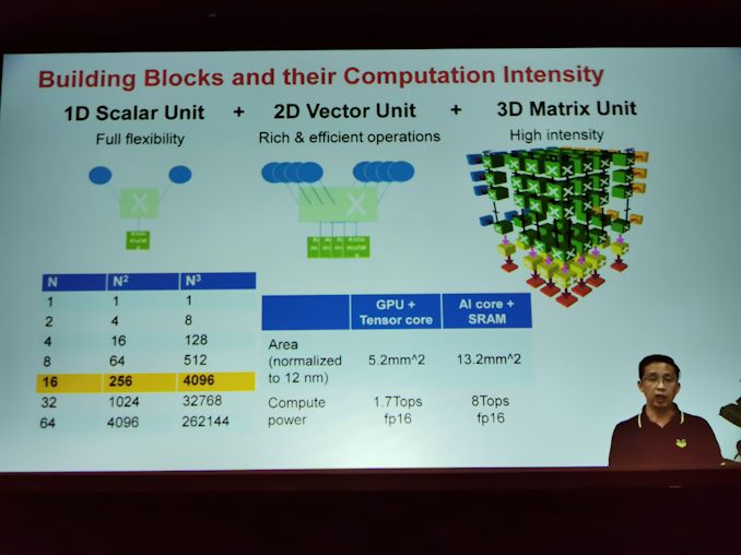
07:53PM EDT - Building Blocks on Da Vinci. 1D, 2D, 3D
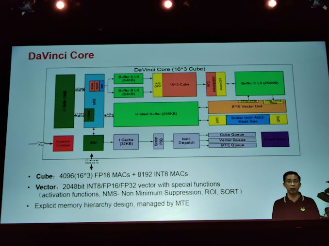
07:54PM EDT - Scalar unit, Vector Unit, and Cube Unit
07:54PM EDT - Cube is 4096 FP15 MACs + 8192 INT8 MACs
07:54PM EDT - L0 buffers for operands
07:54PM EDT - unified buffers
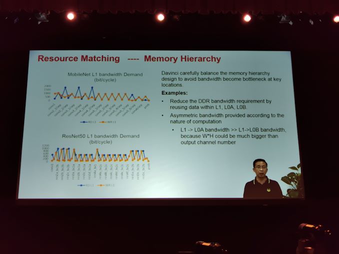
07:54PM EDT - L1 buffer provides the space to reuse data that freuqency cycled through the execution pipeline
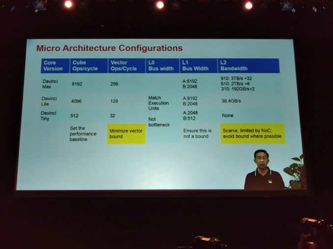
07:55PM EDT - Many versions of the Da Vinci core
07:55PM EDT - Different config of resources for different workloads
07:55PM EDT - Tiny has 512 MACs in a cube, Max has 8192 MACs in a cube
07:55PM EDT - One of the key challenges is balance MACs to L1 width and L2 bandwidth
07:56PM EDT - (Huawei could not make the presentation for various reasons, so the presentation was recorded)
07:56PM EDT - Also balance power
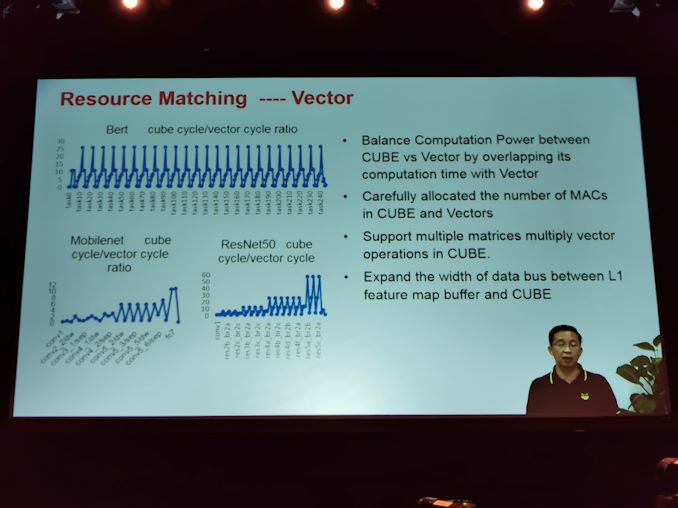
07:56PM EDT - Ratio between vector unit and cube unit varies from layer to layer within a network, and from network to network
07:57PM EDT - Have to make sure the most critical resource is utilized the most
07:57PM EDT - Don't want to be blocked by insufficient resources in other units
07:57PM EDT - Based on cube cycle/vector cycle ratios
07:58PM EDT - Execution time of vector is hidden by execution time of Cube
07:58PM EDT - Need enough bandwidth for the pipeline to prevent stalls
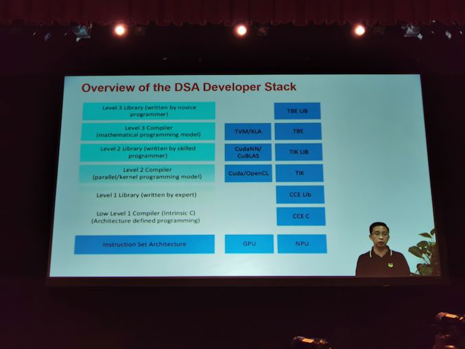
07:59PM EDT - C level programming interface
07:59PM EDT - Multiple level libraries available
07:59PM EDT - This slide shows the different GPU vs NPU
07:59PM EDT - Can go much lower in Da Vinci NPU
07:59PM EDT - But also much higher for entry novice programmers
08:00PM EDT - Designed for everyone
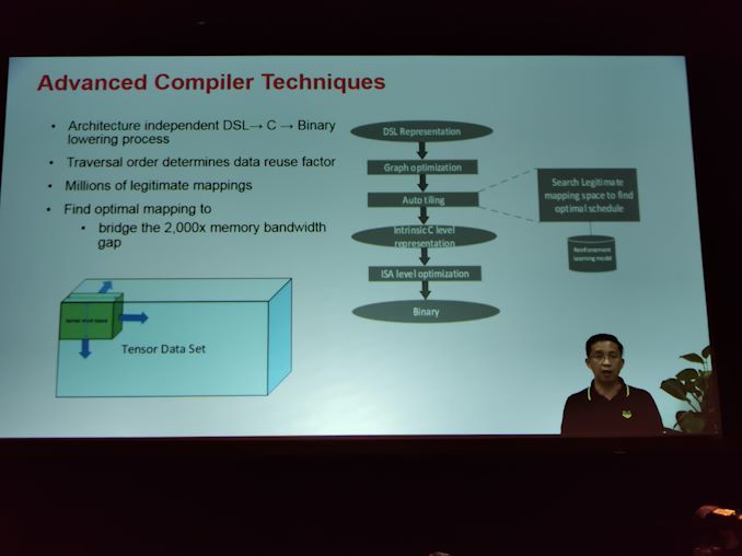
08:00PM EDT - Need advanced compiler techniques
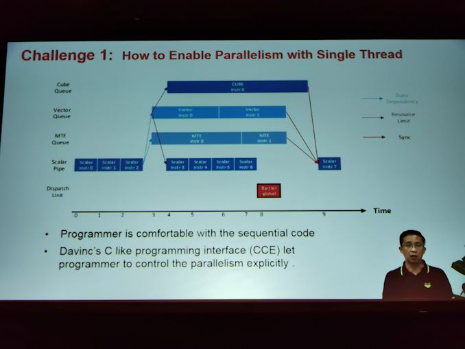
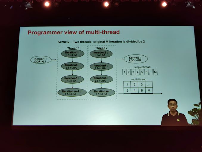
08:00PM EDT - Need to enable parallelism within a single thread
08:01PM EDT - The C level code can extract parallelism with appropriate compiler - HW based multithreading extracted
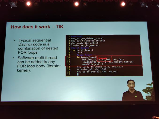
08:02PM EDT - Going deeper, TIK can expended loop bodies due to scheduling
08:04PM EDT - Need advanced compiler techniques for high-level programming
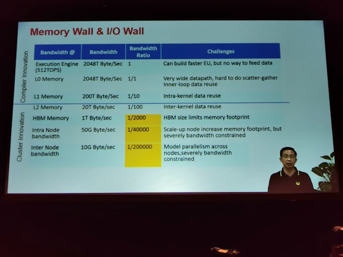
08:04PM EDT - Find optimal mapping to bridge the 2000x memory bandwidth gap
08:04PM EDT - Need to detect the optimum mappings
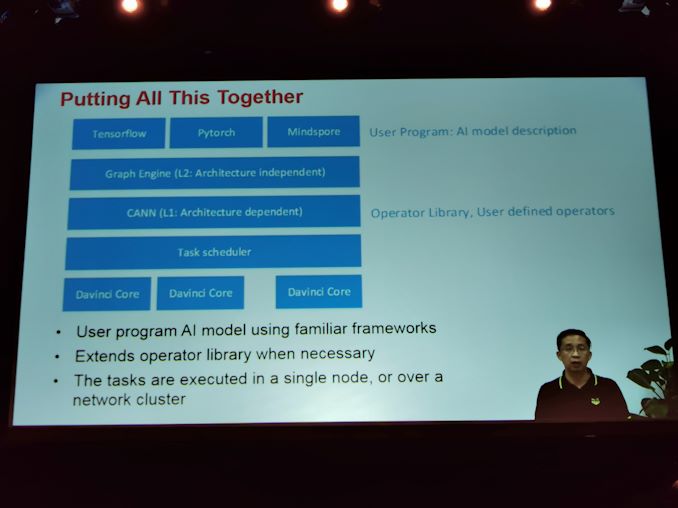
08:05PM EDT - Tensorflow, PyTorch supported. Also custom Huawei called Mindspore
08:05PM EDT - Created a wide range of NPUs built on Davinci
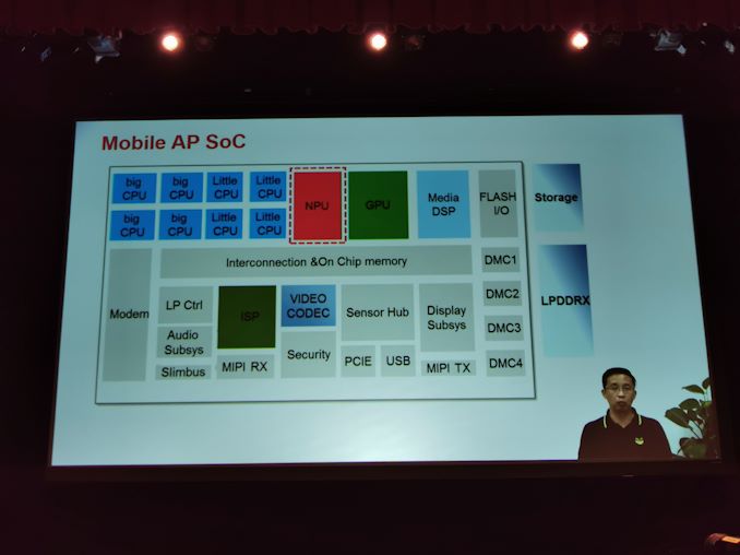
08:05PM EDT - Mobile NPU
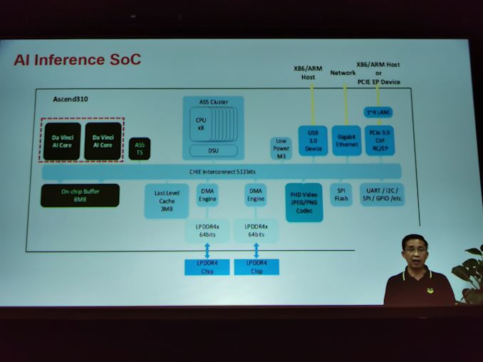
08:06PM EDT - AI Automotive, AI Inference SOC
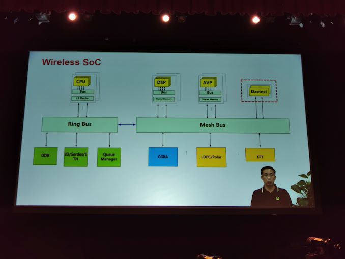
08:06PM EDT - Also Wireless SoCs
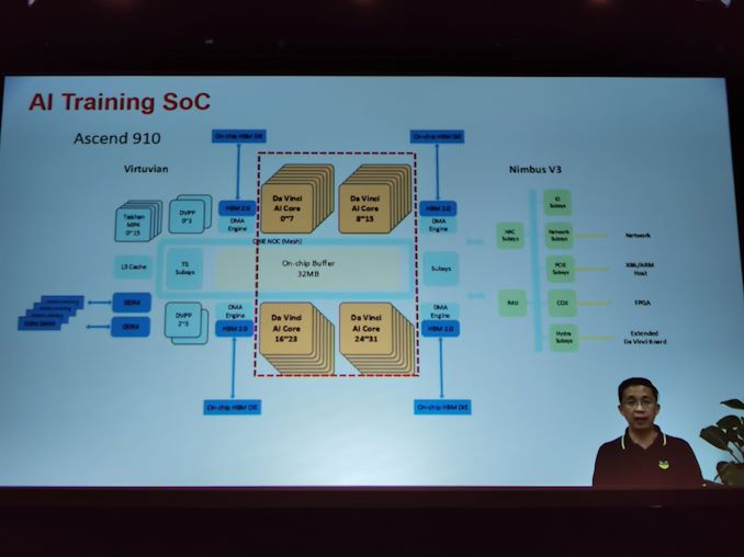
08:06PM EDT - and Training in Ascend 910
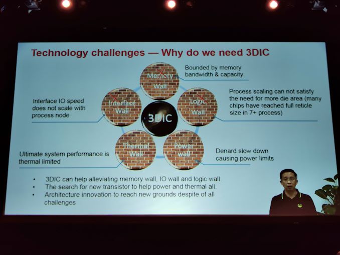
08:07PM EDT - Memory Wall and IO Wall : Even with HBM, 2000:1 gap
08:07PM EDT - Addressed by Multi-Layer cache hierarchy
08:08PM EDT - Also embrace 3DIC
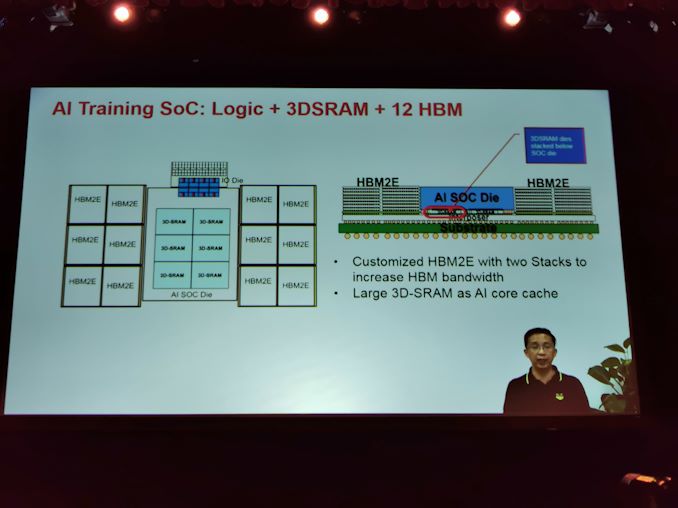
08:08PM EDT - Using 3D stacking technique, allows an increase of bandwidth in memory
08:08PM EDT - Useful die size and heterogenous process node
08:09PM EDT - Future products to increase memory bandwidth and amount of on-chip capacity
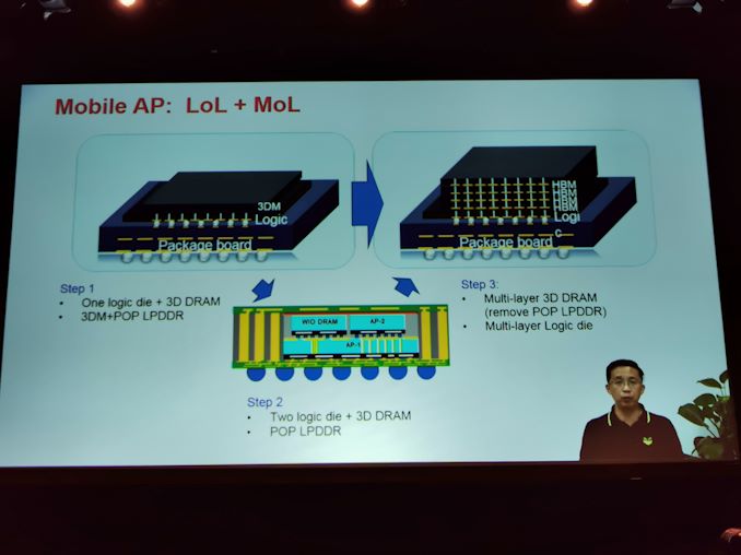
08:09PM EDT - Mobile AP uses different technologies
08:09PM EDT - Multi-Layer logic die
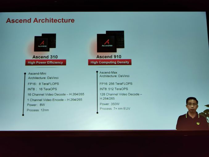
08:10PM EDT - Ascend 310 has 16 TOPs INT8 on 12nm,
08:10PM EDT - Ascend 910 has 512 TOPs at 350W built on 7nm+ EUV
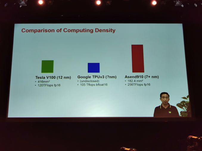
08:11PM EDT - Ascend 910 compared to other compute devices
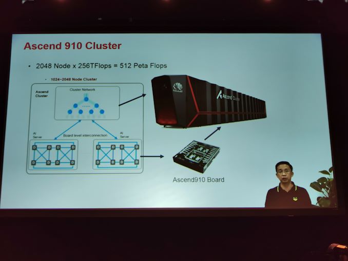
08:11PM EDT - A server with 8 Ascend 910 and two CPU = 6000W
08:12PM EDT - Combine 2048 nodes for 512 PFLOPS
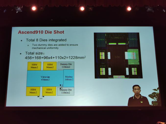
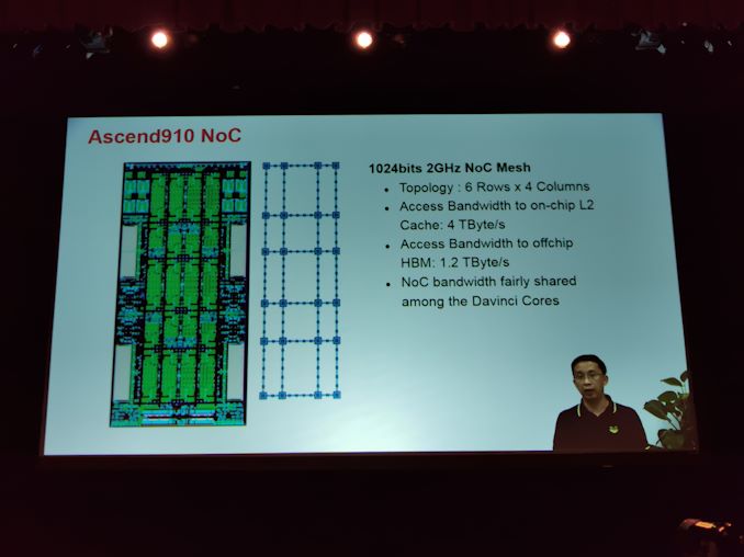
08:12PM EDT - Die shot total 1228 mm2
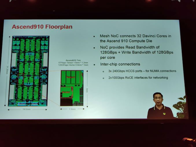
08:12PM EDT - On chip NOC supports 128 GBps R/W per core
08:13PM EDT - 910 has 32 Davinci Cores
08:13PM EDT - Mesh supports 1024-bit 2 GHz NOC
08:13PM EDT - 4 TB/s access to L2
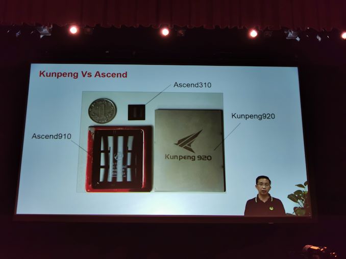
08:14PM EDT - Size of various Ascend Chips next to Kunpeng
08:14PM EDT - THis year, expect to 100m devices with Davinci cores
08:18PM EDT - Q*A
08:18PM EDT - Q: Will you be part of MLperf? A: Await an announcement!
08:20PM EDT - Q: HBM3 offers to double bandiwdth but reduce the size of the stack. How would you deal with this? A: The reach for HBM roadmap is a mjaor issue. If you shorten the reach, you have to put the DRAM on the logic die, which creates the thermal issue. Need a low density interconnect. The bonding technique needs to be improved. The density of wiring needs to be increased. This will create a new opportunity to reduce power. But connected the HBM stack to the main logic die, at the moment it seems like putting HBM on the side is the most practical approach.
08:22PM EDT - Q: Can one architecture cover edge computing and datacenter? A: One of the major emphasis of the design is to make it scalable. Use it in edge and client devices like cell phones and smart cameras, and use the same architecture in the datacenter
08:22PM EDT - Creating the software stack is a big effort so need conformity
08:22PM EDT - That's a wrap. On to the next talk!

