Original Link: https://www.anandtech.com/show/15009/intels-new-atom-microarchitecture-the-tremont-core
Intel's new Atom Microarchitecture: The Tremont Core in Lakefield
by Dr. Ian Cutress on October 24, 2019 1:30 PM EST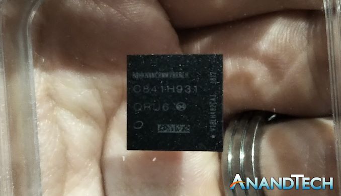
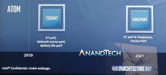
While Intel has been discussing a lot about its mainstream Core microarchitecture, it can become easy to forget that its lower power Atom designs are still prevalent in many commercial verticals. Last year at Intel’s Architecture Summit, the company unveiled an extended roadmap showing the next three generations of Atom following Goldmont Plus: Tremont, Gracemont, and ‘Future Mont’. Tremont is set to be launched this year, coming first in a low powered hybrid x86 design called Lakefield for notebooks, and using a new stacking technology called Foveros built on 10+ nm. At the Linley Processor Conference today, Intel unveiled more about the microarchitecture behind Tremont.
For the sake of clarity, a pre-note on ‘Core’ vs ‘core’:
- ‘Core’ and ‘Atom’ are Intel’s two main x86 microarchitecture families
- A ‘core’ is a single designated CPU capable of processing instructions, and can be built by Intel with either ‘Core’ or ‘Atom’ microarchitectures
A Brief History of Atom
Intel’s lower powered Atom microarchitecture has been used for a variety of solutions: embedded platforms, networking, smartphones, tablets, netbooks, NAS devices, control hubs, and a wide array of things we don’t even know about. The positioning of Atom compared to Core was meant to be that Atom was the smaller core design, taking up less silicon die area and being lower performance, but ultimately lower power in a time where the Core microarchitecture was focused more towards high performance designs.
The last few generations of Atom are readily quantified: Silvermont based on 22nm was a big product for the company, which has evolved into Airmont, Goldmont, Goldmont Plus, and now Tremont.
| Intel's Atom History | ||||||
| AnandTech | Node | Smartphone | Tablet | Netbook Notebook |
Networking Server |
|
| Saltwell | 32nm | 2011 | Medfield Clover Trail+ |
Clover Trail | Cedar Trail | |
| Silvermont | 22nm | 2013 | Merrifield Moorefield |
Bay Trail-T | Bay Trail-M Bay Trail-D |
Rangeley Avoton |
| Airmont | 14nm | 2015 | 'Riverton' | Cherry Trail-T | Braswell | Denverton |
| Goldmont | 14nm | 2016 | 'Broxton' | Willow Trail Apollo Lake |
Apollo Lake | |
| Goldmont+ | 14nm | 2017 | Gemini Lake | |||
| Tremont | 10+ | 2019 | Lakefield | Lakefield | Snow Ridge | |
The Atom family lines get a little confusing with Intel playing in all these spaces. The Atom core within in given family is usually identical (L2 configuration might change), and because of the SoC in play, it might get a different name based on the market where it was headed. Intel scrapped the smartphone program back with Broxton in 2016, and the tablet type of SoC has also gone away. With Lakefield, combining Core and Atom, it could be used in Tablets again for 2019/2020, but we will see it in Notebooks with the Surface Pro Neo and in networking/embedded markets as Snow Ridge.

Lakefield - 12mm x 12mm, 2mW Standby Power
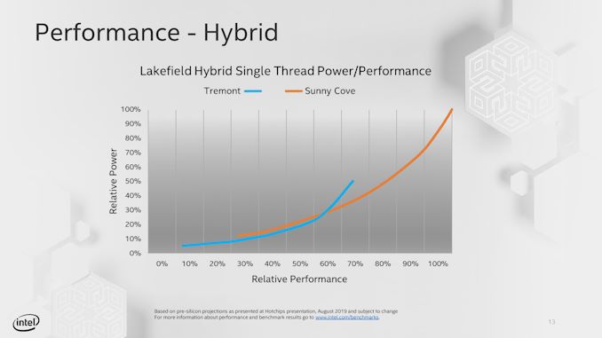
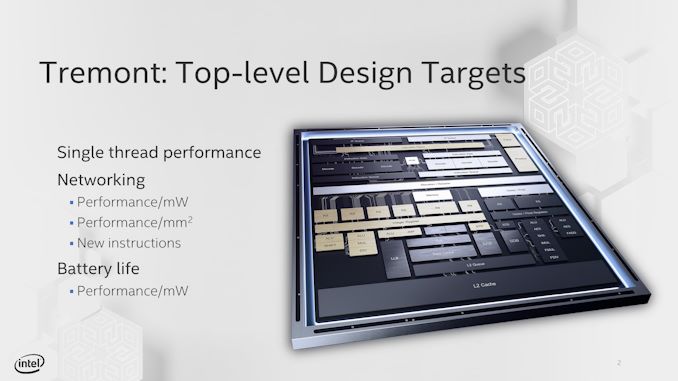
It is worth noting that as Intel expanded the scope of its Core microarchitecture, from 1.5W per core to 20W+ per core, it has kind of edged Atom more into niche products. Atom still had that super-low-power advantage, with a much smaller die area, but has also been super low performance with a quantifiable step-function below what Core can provide. With Tremont, Intel’s primary focus was bringing the single thread performance of the Atom design in parity to Core at the lower end of performance, with a sizeable overlap between the performance of a single Core design against a single Atom design. Intel published this graph to demonstrate what this looks like on early silicon:
Now, Intel’s Atom platforms haven’t had the greatest press over the last few years. Aside from providing some really nice notebooks around the $200 range on the consumer side, the enterprise side has been dealing with a clock degradation issue that ultimately leaves Atom systems built on C2000 processors unable to boot, which was bad news for embedded Atom systems designed to run for 10-20 years. Intel has since fixed that bug with a silicon update, but the point of that silicon was for it not to be touched for a generation.
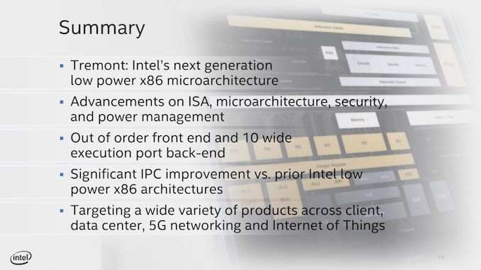
With that aside, Intel is looking to revive its Atom fortunes with the new Tremont design, and looking forward to Gracemont and beyond. More performance, crossing over with Core, and with hardware built on Intel’s latest 10+ process, should afford a number of opportunities. Until we get our hands on the hardware, we’re going to examine the design.
Design Goals for Tremont
The odd quirk about CPU design is that for engineers that have been embedded in this space for 20 years, when they were taught about processor design, the main focus was all about performance. Little attention was paid to power. Fast forward to today, and power is the often talked about point when it comes to battery powered devices, and learning to design for both performance and power becomes an intense balancing act for all the engineers involved. We’ve spoken to companies that only allow performance enhancements if the power increase is at most equal in percentage, or perhaps a 2:1 ratio of performance/power. It’s a difficult pie to bake at any rate.
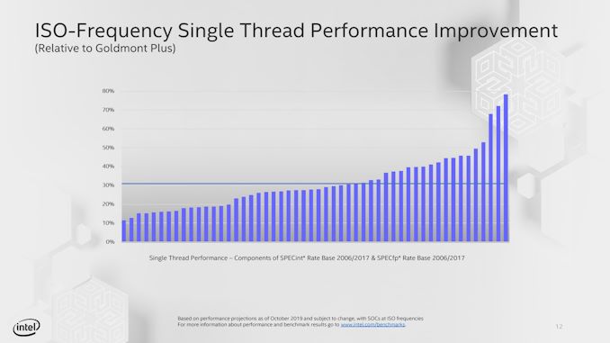
The interesting thing here in our briefing with Intel is that they specifically stated that Tremont was built with performance in mind, and the aim was for a sizeable uptick in the raw clock-for-clock throughput compared to the previous generation Atom, Goldmont Plus. Based on Intel’s own metrics, namely using SPEC, Intel is going to claim an average 30% iso-frequency performance uplift in core performance for Tremont over Goldmont Plus.
It’s worth noting here that this data is from an early Tremont design we were told, and should represent minimum uplifts. The graph is somewhat skewed at the top end with three of the SPEC tests getting 65%+ uplifts, and at the time of discussion, Intel did not have to hand exactly which tests these were (likely libquantum, lbm). We weren’t told how the code was compiled, however Intel did state that the same compiled binaries were used on both Tremont and Goldmont Plus. Intel didn’t state if they’re actually adjusting the clock of each core to match each other, or doing a performance per clock analysis using the frequency as a division factor. These results have to be taken at face value.
A 30% average jump in performance is a sizeable jump for any generation-to-generation cadence. Just taking it as-is feels premature: aside from microarchitectural advancements and a jump to 10nm, there has to be something at play here – either the power budget of Atom has ballooned, or the die area. With Intel explicitly out of the gate stating that their focusing on performance, a cynic is going to suggested that something else has paid that price, and to that end Intel wasn’t prepared to talk about power windows or die area, though they did point to the already announced Lakefield CPU, which has a 1 x Core + 4 x Tremont design and gets compared to 7 W CPUs.
Comparing 14nm Goldmont Plus (that’s standard 14nm, not 14+ or 14++) to a 10+ Tremont core is going to be difficult: the Tremont core has more in it to drive that performance, however what is not known is how much space was saved moving from 14nm to 10+ and if the extra parts make the core bigger or smaller overall. Needless to say, Tremont has more in it to drive that performance, which we’ll cover in the next few pages.
Tremont: A Wider Front End and Caches
For users that have been following our analysis of the Core microarchitecture, it has been hard not to notice that Intel’s design for that family has been, among other things, to continually go wider and wider. This means more instructions in flight, larger caches, bigger buffers, bigger TLBs, more execution ports, and support for more instructions. Going wider isn’t the only thing: the microarchitecture also has to be clever, trying to maximise utilisation, as going wider does nothing for a simple stream of commands.
With Atom, going wider is a key part of the design for Tremont, but Intel has taken a couple of fundamentally different steps to manage exactly what is going on.
A Key Uplift: Fetch and Predict
Another major jump for the Atom microarchitecture are the prefetchers and branch predictors. Intel states that rather than iterate the design from Goldmont Plus, they have transplanted a large part of the prefetchers and branch predictors from the Core design on Sunny Cove. The design isn’t identical according to Intel, due to die area and power concerns, but Intel states that the principles are similar and elements like branch prediction history tables are ‘of the same order’ as the Core design.
Intel states that there is no penalty for an L1 prediction, and that the L2 prediction penalty is smaller than previous generations.
A Key Differentiator: Decode Engines
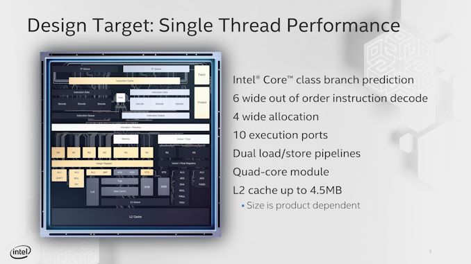
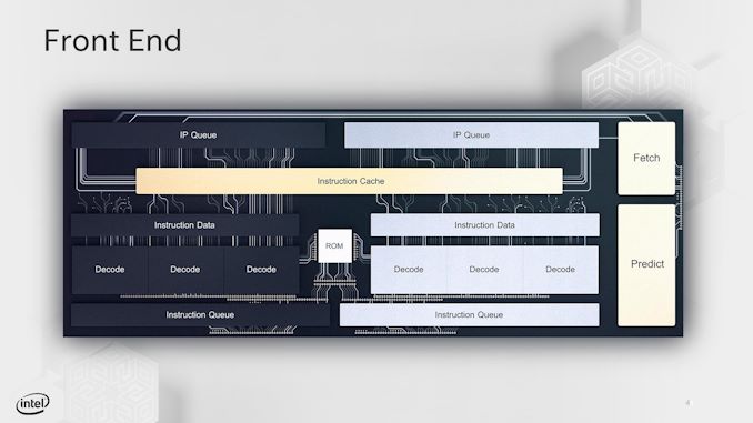
On the face of it, we have a 6-wide decode engine pared with a 4-wide allocation/dispatch engine. This is, on paper, very odd: normally we would expect the decode and dispatch to be equal in width, or at least be able to dispatch more than can be decoded in order to ensure that the re-order buffer doesn’t overflow. With the latest Core microarchitecture, called Sunny Cove, we have a 4-to-6 wide decode that also supports a micro-op cache, which all leads into a large reorder buffer and a 10-wide dispatch to the back-end. Tremont is, by contrast, has the opposite ratio.
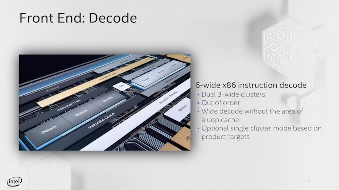
Saying that this is a 6-wide decode engine is actually slightly incorrect. What Intel has done here is split the decode into dual 3-wide engines instead.
Each decode engine, when dealing with different branch predictions, can take a separate instruction stream. This allows for a higher average utilization across both of the 3-wide decode engines compared to a single 6-wide engine, but when a branch isn’t present it means that one of the decode engines can be clock gated to save power. For a single instruction stream, the Tremont design is actually only 3-wide decode, with a 4-wide dispatch.
(Technically Intel states that, through microcode, they can change the decode engines to act as a single 6-wide implementation rather than dual 3-wide engines. This won’t be configurable to the OEM, but based on demand Intel may make specific products for customers that request it.)
So just to clarify, Tremont does not have a micro-op cache. When discussing with Intel about the benefits of this dual decode engine design compared to having a micro-op cache, Intel stated that a micro-op cache can help utilize a wide-decode design better, but with a smaller per-engine decode size, they were able to see a performance uplift as well as save die area by using this dual-engine design. Intel declined to comment which one was better, but we were told that given the die size, power envelope of Atom, and the typical instruction flow of an Atom core, this design yielded the better combination of performance, power, and area.
Another improvement for Intel after the decode engines is the re-order buffer. Intel states that it can support 208 instructions, compared to 78 in Goldmont and 95 in Goldmont Plus, which is a sizeable uplift. Intel did not specify if Tremont has the ability to fuse instructions into micro-ops for the ROB (Goldmont did not), however there is a near 1:1 parity of instructions to micro-ops we were told.
Caches
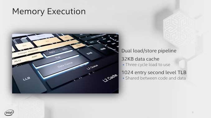
Intel has also increased the size of its L1 data cache. The L1 instruction cache says at 32 KiB/core with 8-way associativity, but ever since the 22nm era, Intel has kept a 24 KiB/core L1 data cache on its Atom design. With Tremont, both the L1-I and L1-D are now a 32 KiB/core design with 8-way associativity. Intel states that its L1 data cache here has a 3-cycle latency, compared to Skylake which has a 32 KiB L1D at a 4-cycle latency, or Sunny Cove which has a 48 KiB L1D at a 5-cycle latency.
| Intel Caches | ||||||
| AnandTech | Tremont | Goldmont+ | Goldmont | Sunny Cove | Skylake | |
| Process | 10+ | 14 | 14 | 10+ | 14++ | |
| Decode | 2x3-wide | 3-wide | 3-wide | 4-6 wide | 4-5 wide | |
| Allocate | 4-wide | 4-wide | 3-wide | 10-wide | 8-wide | |
| L1 Instruction | 32 KiB/Core 8-way |
32 KiB/Core 8-way |
32 KiB/Core 8-way |
32 KiB/Core 8-way |
32 KiB/Core 8-way |
|
| L1 Data | 32 KiB/Core 8-way |
24 KiB/Core 6-way |
24 KiB/Core 6-way |
48 KiB/Core 12-way |
32 KiB/Core 8-way |
|
| L1 Latency | 3-cycle | 3-cycle | 3-cycle | 5-cycle | 4-cycle | |
| L2 Cache | 1.5-4.5 MiB Per Module 12-18 way |
1.0 MiB Per Core 16-way |
0.5-1.0 MiB Per Core 16-way |
512 KiB Per Core 8-way |
256 KiB Per Core 4-way |
|
| L2 Latency | 17-cycle | 19-cycle | 17-cycle | 13-cycle | 12 cycle | |
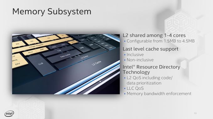
For the L2 cache, for most Atom cores in the past, this has essentially been a last-level cache split across all cores in a ‘module’. Depending on the generation will depend on the size of the module: for 22nm Silvermont, we saw an L2 cache of 512 KiB/core, which was increased with Goldmont up to 1.0 MB/core. With Tremont, Intel has specified that L2 will vary depending on the product, from 1.5 MiB to 4.5 MiB per module. A module for Tremont will be anything up to four cores, so we could see designs with a single core featuring 4.5 MiB of L2 cache, or a quad-core design with 1.5 MiB of L2. Within a module, all cores have access to the cache, however a core will not have access to the L2 in a different module. The L2 can be set through microcode as an inclusive or a non-inclusive cache.
Intel states that the L2 cache has an average 17-cycle latency, and the associativity will be a function of the size: 1.5 MB will be a 12-way design, while 4.5 MB will be an 18-way design. (We therefore assume that a 3.0 MB L2 will be 15-way.)
Tremont also adds support for a global L3 cache across modules. Both the L2 and L3 cache support QoS arrangements, allowing for data prioritization and memory bandwidth enforcement for specific threads or virtual machines. This is a technology that Intel introduced with Broadwell Xeons to help avoid ‘noisy neighbor’ environments in data centers.
A Wider Back End
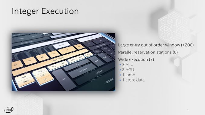
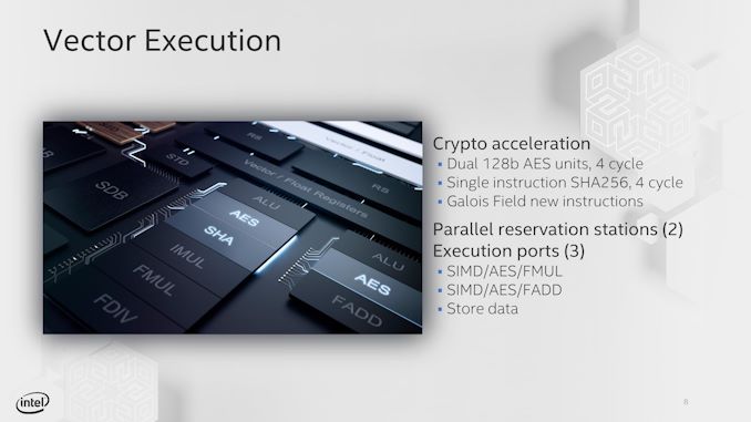
Moving beyond the micro-op queue, Tremont has an 8 execution ports, filled from 7 reservation stations.
The only two ports using a combined reservation station are the address generator units (AGUs) - this is in stark contrast to the Core design, which in Sunny Cove uses a unified reservation for all integer and floating point calculations and three for the AGUs. The reason that Tremont uses a unified reservation station for the two AGUs, also backed by extra memory for queued micro-ops, is in order to supply both AGUs with either 2x 16-byte stores, 2x 16-byte loads, or one of each. Intel clearly expects the AGUs on Tremont to be fairly active compared to other execution ports.
On the integer side, aside from the two AGUs, Tremont has 3 ALUs, a jump port, and a store data port. Each ALU supports different functions, with one enabling shift functions and another for multiplication and division. Compared to core, these ALUs are extremely lightweight, and Intel hasn’t gone into specifics here.
On the floating point side, we are a little bit more varied – the three ports are split between two ALUs and a store port. The two ALUs have one focused on fused additions (FADD), while the other focuses on fused multiplication and division (FMUL). Both ALUs support 128-bit SIMD and 128-bit AES instructions with a 4-cycle latency, as well as single instruction SHA256 at 4-cycles. There is no 256-bit vector support here. In order to help with certain calculations, GFNI instruction support is included.
There is also a larger 1024-entry L2 TLB, supporting 1024x 4K entries, 32x 2M entries, or 8x 1G entries. This is an upgrade from the 512-entry L2 TLB in Goldmont.
New Instructions
As with any generation, Intel adds new supported instructions to either accelerate common calculations that would traditionally require lots of instructions or to add new functionality. Tremont is no different.
| TITLE | |||||
| AnandTech | Tremont | Goldmont Plus |
Goldmont | Airmont | Silvermont |
| Process | 10+ | 14 | 14 | 14 | 22 |
| Release Year | 2019 | 2017 | 2016 | 2015 | 2013 |
| New Instructions | CLWB GFNI ENCLV CLDEMOTE MOVDIR* TPAUSE UMONITOR UWAIT |
SGX1 UMIP PTWRITE RDPID |
RDSEED SMAP MPX XSAVEC XSAVES CLFLUSHOPT SHA |
SSE4.1 SSE4.2 MOVBE CRC32 POPCNT CLMUL AES RDRAND PREFETCHW |
|
(When asked what other new instructions are supported, Intel stated to look at the published documents about future instructions. When it was pointed out that those documents weren’t exactly clear and that in the past Intel hasn’t spoken about future designs, we were not afforded additional comments.)
When we get hold of a Tremont device, we’ll do a full instruction breakdown.
Beyond the Core
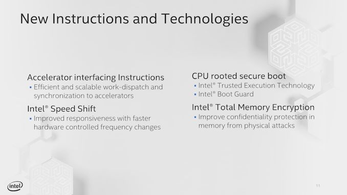
Nominally today’s disclosure is more about the Tremont microarchitecture than any SoC it might appear in, like Lakefield or Snow Ridge. To that end, Intel wasn’t talking about GPU support (Lakefield will have Gen11 graphics), but Intel did discuss that Tremont would be the first Atom design to fully support Intel’s Speed Shift / ACPI hardware flags, allowing for faster ramp-up and ramp-down of high-frequency operation.
Intel also stated that Tremont supports Total Memory Encryption to prevent physical attacks, Rooted Secure Boot and Boot Guard, and specific accelerator interfacing instructions. With respect to Spectre, Meltdown, and L1TF, Intel stated that Tremont will have the same protections as Cascade Lake.
We also asked Intel about module-level voltage and power control. We were told that within a quad-core module with four Tremont cores, all the cores share the same frequency plane, but each core can enter separate c-states to reduce power consumption when not in use.
Final Thoughts and Slide Deck
In the past, at least from my perspective, dealing with Atom platforms has been amusing. Atom devices typically work great for hyper-focused and optimized software that can take advantage of a latency-insensitive workload, such as networking equipment or a NAS, but for any general purpose use I find them incredibly slow. Perhaps I’m just too used to the big cores on the devices I use – but with Intel saying that Atom is being refocused on performance, it will be interesting to see how Tremont devices and other Core devices will overlap. This graph from Intel is very striking, and if you squint, it looks a lot like some of the smartphone power/performance graphs we’ve produced in the past.
With Intel moving Core down in power to the 1.5W level, again it will be interesting to see how Tremont can play in that 2mW to 2W range that Atom has traditionally played in. The last generation Goldmont Plus devices were going beyond that, and in this power range we also have smartphone cores coming into play. After showing the slide deck to Andrei, we were discussing how a Tremont might stack up against an Arm Cortex A76, or a Kryo core. When we can get our hands on Tremont, we’ll see how they compare. When it comes to the products that Tremont is aiming for however, it still has that x86 advantage.
We did ask a few questions from Intel that we didn’t get answers to, such as die size and target frequencies. The other question to discuss is Intel’s current high-demand issues putting pressure on its manufacturing technologies. Tremont is still a low cost, low powered core, so logic may dictate that it will be a while before we see consumer chips enter the market. Ultimately Intel’s high-demand issues are around 14nm, and so far we’ve only seen Tremont discussed on Intel’s 10+ process with Lakefield and Snow Ridge. What we know about Intel’s 10nm/10+ capacity isn’t a lot, but reports vary from yields being ‘on track’ to ‘working with key OEM partners only’. Intel’s driver for 10+ right now is Ice Lake, which is coming to some premium notebook designs this year, and Lakefield has been announced for the Surface Neo. It is not known what the expected volume for the Neo will be, but it is unlikely to be large. Whether or not Tremont will see the light of day in traditional Atom Celeron and Pentium processors is another question entirely – the Goldmont Atom families have suffered while Intel’s 14nm efforts are more focused on enterprise hardware that can be sold for a much higher $$ per square millimeter. Beyond Lakefield, we might not actually see Tremont in any other consumer chip before the next generation Atom if Intel cannot get its issues sorted.
As and when we get a Lakefield device, we will put it through our tests. Stay tuned.

