Original Link: https://www.anandtech.com/show/16084/intel-tiger-lake-review-deep-dive-core-11th-gen
Intel’s Tiger Lake 11th Gen Core i7-1185G7 Review and Deep Dive: Baskin’ for the Exotic
by Dr. Ian Cutress & Andrei Frumusanu on September 17, 2020 9:35 AM EST- Posted in
- CPUs
- Intel
- 10nm
- Tiger Lake
- Xe-LP
- Willow Cove
- SuperFin
- 11th Gen
- i7-1185G7
- Tiger King

The big notebook launch for Intel this year is Tiger Lake, its upcoming 10nm platform designed to pair a new graphics architecture with a nice high frequency for the performance that customers in this space require. Over the past few weeks, we’ve covered the microarchitecture as presented by Intel at its latest Intel Architecture Day 2020, as well as the formal launch of the new platform in early September. The missing piece of the puzzle was actually testing it, to see if it can match the very progressive platform currently offered by AMD’s Ryzen Mobile. Today is that review, with one of Intel’s reference design laptops.
Like a Tiger Carving Through The Ice
The system we have to hand is one of Intel’s Reference Design systems, which is very similar to the Software Development System (SDS) we tested for Ice Lake last year. The notebook we were sent was built in conjunction with one of Intel’s OEM partners, and is meant to act as an example system to other OEMs. This is slightly different to the software development system, which was mainly for the big company software developers (think Adobe) for code optimization, but the principle is still the same: a high powered system overbuilt for thermals and strong fans. These systems aren’t retail, and so noise and battery life aren’t part of the equation of our testing, but it also means that the performance we test should be some of the best the platform has to offer.
Our reference design review sample implements Intel’s top tier Tiger Lake ‘Core 11th Gen’ processor, the Core i7-1185G7. This is a quad core processor with hyperthreading, offering eight threads total. This processor also has the full sized new Xe-LP graphics, with 96 execution units running up to 1450 MHz.
I haven’t mentioned the processor frequency or the power consumption, because for this generation Intel is deciding to offer its mobile processors with a range of supported speeds and feeds. To complicate the issue, Intel by definition is only publically offering it in the mix-max form, whereas those of us who are interested in the data would much rather see a sliding scale.
| Intel Core i7-1185G7 'Tiger Lake' | |
| Cores Threads |
4 Cores 8 Threads |
| Base Frequency at 12 W | 1200 MHz |
| Base Frequency at 15 W | 1800 MHz |
| Base Frequency at 28 W | 3000 MHz |
| 1C Turbo up to 50 W | 4800 MHz |
| All-core Turbo up to 50 W | 4300 MHz |
| L2 Cache | 1.25 MB per core (non-inclusive) |
| L3 Cache | 12 MB (non-inclusive) |
| Integrated Graphics | Xe-LP 96 Execution Units 1350 MHz Turbo |
| Memory Support | 32 GB LPDDR4X-4266 or 64 GB DDR4-3200 |
In this case, the Core i7-1185G7 will be offered to OEMs with thermal design points (TDPs) from 12 W to 28 W. An OEM can choose the minimum, the maximum, or something in-between, and one of the annoying things about this is that as a user, without equipment measuring the CPU power, you will not be able to tell, as the OEMs do not give the resellers this information when promoting the notebooks.
For this reference design, it has been built to offer both, so in effect it is more like a 28 W design for peak performance as to avoid any thermal issues.
At 12 W, Intel lists a base frequency of 1.2 GHz, while at 28 W, Intel lists a base frequency of 3.0 GHz. Unfortunately Intel does not list the value that we think is most valuable – 15 W – which would enable fairer comparisons with the previous generation Intel hardware as well as the competition. After testing the laptop, we can confirm that the 15 W value as programmed into the silicon (so we’re baffled why Intel wouldn’t tell us) is 1.8 GHz.
In both 12 W and 28 W scenarios, the processor can turbo up to 4.8 GHz on one core / two threads. This system was built for thermals or power to not to be an issue, so the CPU can boost to 4.8 GHz in both modes. Not only that, but the power consumption while in the turbo modes is limited to 55 W, for any TDP setting. The turbo budget for the system increases with the thermal design point of the processor, and so when in 28 W mode, it will also turbo for longer. We observed this in our testing, and you can find the results in the power section of this review.
The Reference Design
Intel sampled its Reference Design to a number of the press for testing. We had approximately 4 days with the device before it had to be handed back, enough to cover some key areas such as best-case performance on CPU and GPU, microarchitectural changes to the core and cache structure, and some industry standard benchmarks.
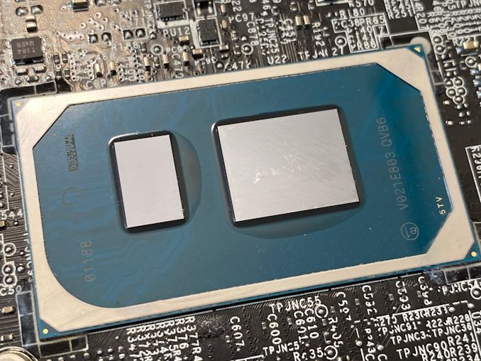
There were some caveats and pre-conditions to this review, similar to our initial Ice Lake development system test, because this isn’t a retail device. The fans were fully on and the screen was on a fixed brightness. Intel also requested no battery life testing, because the system hasn't been optimized for power in the same way a retail device would - however as we only had a 4 day review loan, that meant that battery life testing wasn’t possible anyway. Intel also requested no photography of the inside of the chassis, because again this wasn’t an optimized retail device. The silicon photographs you see in this review have been provided by Intel .
When Intel’s regional PR teams started teasing the reference design on twitter (e.g. UK, FR), I initially thought this was an Honor based system due to the blue chamfered bezel like the Magicbook I reviewed earlier in the year. This isn’t an Honor machine, but rather one of the bigger OEMs known for its mix of business and gaming designs.
Large keypad, chiclet style keys, and a 1080p display. For ports, this design only has two Type-C, both of which can be used for power or DisplayPort-over-Type C. The design uses the opening of the display to act as a stand for the main body of the machine.
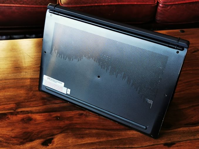
On the back is a big vent for the airflow in. Under the conditions of the review sample we’re not able to take pictures of the insides, however it’s clear that this system was built with an extra dGPU in mind. Intel wasn’t able to comment on whether the OEM it partnered with will use this as a final design for any of its systems, given some of the extra elements added to the design to enable its use as a reference platform.
For the full system build, it was equipped with Intel’s AX201 Wi-Fi 6 module, as well as a PCIe 3.0 x4 Samsung SSD.
| Intel Reference Design: Tiger Lake | |
| CPU | Intel Core i7-1185G7 Four Cores, Eight Threads 1200 MHz Base at 12 W 1800 MHz Base at 15 W 3000 MHz Base at 28 W 4800 MHz Turbo 1C up to 50W 4300 MHz Turbo nT up to 50W |
| GPU | Integrated Xe-LP Graphics 96 Execution Units, up to 1450 MHz |
| DRAM | 16 GB of LPDDR4X-4266 CL36 |
| Storage | Samsung 1 TB NVMe PCIe 3.0 x4 SSD |
| Display | 14-inch 1920x1080, Fixed Brightness |
| IO | Two Type-C ports Supporting Charge, DP over Type-C |
| Wi-Fi | Intel AX201 Wi-Fi 6 CNVi RF Module |
| Power Modes | 15 W, no Adaptix 28 W, no Adaptix 28W, with Adaptix |
| Others | Battery Speakers Fingerprint Sensor |
The first devices to market with the Core i7-1185G7 will have either LPDDR4X-4266 (32 GB) or DDR4-3200 (64 GB). Intel advertised these chips also supporting LPDDR5-5400, and we confirmed with the engineers that this initial silicon revision is built for LPDDR5, however it is still in the process to be validated. Coupled with the high cost of LPDDR5, Intel expects LP5 systems a bit later in the product cycle life-time, probably in Q1 2021.
On storage: Tiger Lake technically supports PCIe 4.0 x4 from the processor. This can be used for a GPU or SSD, but Intel sees it mostly for fast storage. Given the prevalence of PCIe 4.0 SSDs on the market already, it was curious to see the reference designs without a corresponding PCIe 4.0 drive. Intel’s official reason for not equipping the system with such a drive was along the lines of ‘they’ve not been in the market for long and so we weren’t able to validate in time’. This is immediately and painfully laughable – PCIe 4.0 x4 enabled drives, built on Phison’s E16 controller, have been in the market for six months. We reported on them last year at Computex. To be clear, Intel’s argument here isn’t simply that it didn’t have enough time to validate it, it is the combination of validation time plus the argument that the drives haven’t been out in the market long enough for validation. This is wrong. If the drives had only been in the market for 6-8 weeks, perhaps I might agree with them, but to say it when the drives have been out for 24+ weeks amazes me.
The real reason why this system doesn’t have a PCIe 4.0 x4 drive is because the E16 drives are too power hungry. The E16 is based on Phison’s E12 PCIe 3.0 SSD controller, but with the PCIe 3.0 removed and PCIe 4.0 added, without much adjustment to the compute side of the controller or the efficiency point of the silicon. As a result, the E16-based drives can score up to 8 W for a peak throughput of 5 GB/s. A properly designed from-the-ground-up PCIe 4.0 x4 drive should be able to reach 8 GB/s at theoretical peak, preferably in that 2-4 W window.
Adding an 8 W PCIe 4.0 SSD to a notebook, as we’ve said since they were launched, is a bad idea. Most laptops don’t have the cooling requirements for such a power hungry SSD, causing hot spots and thermal overrun, but also the effect on battery life would be easily noticeable. If Intel had said that ‘current PCIe 4.0 x4 drives on the market aren’t suitable due to the high power consumption of current solutions, however future drives will be much more suitable’, I would have agreed with them as a valid reason for not using one in the reference design. It makes sense – it certainly makes more sense than the reason first given about not being in the market long enough for validation.
Beyond all this, by the time Tiger Lake notebooks come to market, new drives built on Phison’s E18 and Samsung’s Elpis PCIe 4.0 controllers are likely to be available. Whether these will be available in sufficient numbers for notebook deployment would be an interesting question, and so we are likely to see a mix of PCIe 3.0 and PCIe 4.0 enabled NVMe SSDs. I’m hopeful the OEMs and resellers will identify which are being used at the point of sale, or offer different SKU variants between PCIe 3.0 and PCIe 4.0, but I wouldn’t put money on it.
Priority on Power
Normal operation on a notebook is for the processor to be offered at a specific thermal design point, and any changes to the power plan in the operating system will affect how long the system uses its turbo mode, or requirements to enter higher power states. This is because most notebooks are built to be optimized around that single thermal design point.
In our Ice Lake development system (and in a few select OEM designs, like the Razer Stealth), the power slider while in the ‘Balanced’ power mode allowed us to choose between a 15 W power mode and a 25 W power mode, adjusting the base frequency (and subsequently the turbo budget) of the processor. The chassis was built for the higher power modes, and it allowed anyone using the development system to see the effect of the performance between the two thermal design points.
For our Tiger Lake reference design, we have a similar adjustment at play. The power slider can choose either 15 W mode or 28 W mode (note that this is different to the 12 W to 28 W mode that Intel’s Tiger Lake is meant to offer, which I found odd for leaving out, but good in the sense that we could do 15W to 15W comparisons). There is also a third option: 28 W with Intel’s Dynamic Tuning enabled, also known as Adaptix.
Intel’s Dynamic Tuning/Adaptix is a way for the system to more carefully manage turbo power and power limits based on the workload at hand. With Adaptix enabled, the idea is that the power can be more intelligently managed, giving a longer turbo profile, as well as a better all-core extended turbo where the chassis is capable. Intel has always stated that Adaptix is an OEM-level optimization, and it wasn’t enabled in our Ice Lake testing system due to that system not being optimized in the same way.
However for our Tiger Lake system it has been enabled - at least in the 28 W mode anyway. Technically Adaptix could be enabled at any thermal design point, even at 12 W, but in all cases it should offer better performance in line with what the chassis can provide and the OEM feels safe. It still remains an OEM-enabled optimization tool, and Intel believes that the 28 W with Adaptix mode on the reference design should showcase Tiger Lake in its best light.
More info later in the review.
This Review
As a first look at Tiger Lake’s performance, our goal with this review is to confirm the claims Intel has made. The new platform has new features, and Intel has promoted its performance against the competition and previous generation. We’ll also go into microarchitectural details.
Page two will be a brief primer on the fundamental updates on Tiger Lake: the transition to 10nm ‘SuperFin’ technology, the enhanced frequency, and the graphics. We’ll also cover the core as compared to Ice Lake, as well as the SoC level changes such as cache and updated hardware blocks.
We’ll then move onto the new data. Page three will cover the minor changes in the core when it comes to instructions, as well as updates to security. We’ll also cover cache performance, latency, and a key part of modern computing in frequency ramping on page four.
For the power consumption part of the coverage, I’m going to cover it into two brackets: how Intel compares to its own previous generation at 15 W, then moving onto the difference between a 15 W Tiger Lake and a 28 W Tiger Lake, which is going to be a running theme throughout this review.
In Intel’s own announcement for Tiger Lake, the company pitted the 28 W version of Tiger Lake against the best power and thermal setting on an AMD 15 W processor; we’re going to see if those performance comparisons actually hold water, or if it’s simply a diversionary tactic to show Intel has the upper hand by using almost 2x the power.
We’ll also cover our CPU gaming benchmark suite, tested at both 1080p maximum as well as 720p minimum. Intel made big claims about its new Xe-LP graphics architecture against AMD, so we will see how these measure up, both in 15 W Tiger Lake and 28 W Tiger Lake modes.
Pages
- Tiger Lake: Playing with Toe Beans
- 10nm Superfin, Willow Cove, Xe, and new SoC
- New Instructions and Updated Security
- Cache Performance, Core-to-Core Latency, and Frequency Ramping
- Power Consumption: Comparing 15 W TGL to 15 W ICL
- Power Consumption: Comparing 15 W TGL to 28 W TGL
- CPU Performance: SPEC 2006, SPEC 2017
- CPU Performance: Office and Web
- CPU Performance: Simulation and Science
- CPU Performance: Encoding and Rendering
- CPU Performance: Legacy and Synthetic
- Xe-LP GPU Performance: Borderlands 3, Gears Tactics
- Xe-LP GPU Performance: Final Fantasy XIV, Final Fantasy XV
- Xe-LP GPU Performance: Civilization 6, Deus Ex Mankind Divided
- Xe-LP GPU Performance: World of Tanks, Strange Brigade
- Conclusion: Is Intel Smothering AMD in Sardine Oil?
10nm SuperFin, Willow Cove, Xe, and new SoC
Inside Intel’s 11th Generation ‘Tiger Lake’ processor are four ‘Willow Cove’ cores, 96 Execution Units of graphics built with the Xe-LP microarchitecture, all on top of Intel’s latest 10nm SuperFin manufacturing technology. Because each part of this processor has had updates, even trying to explain it in a single sentence can be cumbersome. For the most part, Intel has covered a number of details relating to all these features across the events in August and September – at Intel’s Architecture Day 2020 and the 11th Gen Core announcement, which we will recap here before going into our own testing.
Our full articles on this information can be found at:
- Intel’s 11th Gen Core Tiger Lake SoC Detailed: SuperFin, Willow Cove and Xe-LP
- Intel Launches 11th Gen Core Tiger Lake: Up to 4.8 GHz
10nm SuperFin
Intel’s Tiger Lake design has been enabled through its latest manufacturing process node update. This is a new version of Intel’s 10nm process, and Intel claims that this update is akin to a ‘full node transition’, as if Intel was offering a new manufacturing process altogether. To back up this claim, Intel says that the new generation 10nm offers 17-18% better transistor performance compared to the previous generation 10nm, equivalent to the four updates it applied to 14nm over several years but at the same time. This is a good thing – better performance, a wider frequency and voltage window, and potentially better density, all while using the same manufacturing hardware.
Intel is calling its new process node enhancement ‘SuperFin’, based two of the key design changes that the company has used.
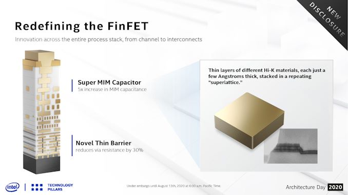
At the lower layers of the stack, Intel is introducing a new set of barrier materials to enable thinner barriers, which also helps reduce resistance of vias by up to 30% by enabling the metal each via to be a bigger proportion of the fixed size. Reducing the resistance enhances the performance of the interconnect between the metal layers
At the higher levels, Intel is introducing a new SuperMIM (metal-insulator-metal) capacitor. Intel states that this new design gives a 5x increase in capacitance over an industry standard MIM cap within the same footprint. This drives a voltage reduction that ultimately leads to drastically improved product and transistor performance. Intel states that this is an industry first/leading design, enabled through careful deposition of new Hi-K materials in thin layers, smaller than 0.1nm, to form a superlattice between two or more material types.
On top of this, a new high-performance third generation FinFET design, enabled through a better gate-generation process and lower resistance source/drain, is what Intel has stated will enable future products. All combined, against a base 10nm process (Intel doesn’t specify which, although most analysts assume this is Cannon Lake, the OG 10nm), Intel is promoting 17-18% better transistor performance with the SuperFin.
Going forward, all products built on this process are going to be called ‘10nm SuperFin’. In the original 10nm parlance, this was 10++. Note that 10++ was renamed 10+ back at CES 2020, and so this is the second renaming. To avoid any confusion, Intel has provided a decoder ring to keep everyone up to date:
- (Pre-10nm: Cannon Lake)
- 10nm: Ice Lake Notebook, Ice Lake Xeon, Snow Ridge
- 10nm SuperFin: Tiger Lake, Xe-LP Products (DG1, SG1)
- 10nm Enhanced Superfin: Sapphire Rapids Xeon, Xe-HP Products (1-4 Tile)
After 10ESF we should see Intel move into its 7nm process and products.
Tiger Lake: Willow Cove
The new microarchitecture of the main CPU cores is called Willow Cove, and is an update over the previous generation Sunny Cove. Intel claims a 10-20% performance improvement generation on generation, however it is important to understand that this is not a raw clock-for-clock gain but rather a peak performance claim.
In terms of a clock-for-clock gain, Intel by and large has said in our technical briefings that Willow Cove will only have minor improvements due to the cache structure (more on that below). Aside from the cache, there are a few changes to deal with security and side-channel attacks, but no other changes to the core design to note. We did discover a few performance updates to specific instructions, which we’ll go into later in the review, but essentially unless the core is L2/L3 cache sensitive, users should not expect to see a clock-for-clock performance difference.
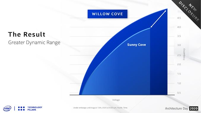
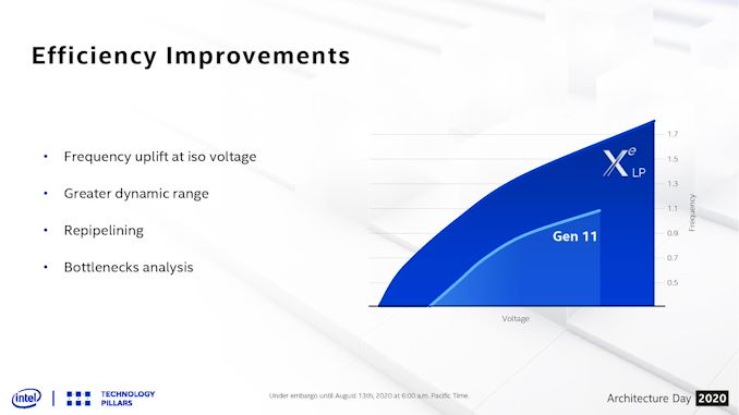
Where Tiger Lake’s 10-20% performance uplift comes from is both performance efficiency and peak performance. Because of the SuperFin design, and a new high-performance transistor library, Intel claims to have enabled the Willow Cove core to be more efficient at every frequency compared to the previous generation, but also extend the frequency range. Where the previous generation was limited to around 4.0 GHz, the new Tiger Lake as launched can go to 4.8 GHz. Based on our discussions with Intel’s engineers, it can go even higher.
Aside from the frequency adjustment, the biggest change inside the core is the cache hierarchy.
The private L2 cache gets the biggest update, with a +150% increase in size. Traditionally increasing the cache size by double will decrease the miss rate by √2, so the 2.5x increase should reduce L2 cache misses by ~58%. The flip side of this is that larger caches often have longer access latencies, so we would expect the new L2 to be slightly slower. After many requests, Intel said that its L2 cache was a 14-cycle latency, which we can confirm, making it only +1 cycle over the previous generation. It’s quite impressive to more than double a cache size and only add one cycle of latency. The cache is also now a non-inclusive cache.
The L3 also gets an update, in two ways. The size has increased for the highest core count processors, from 2 MB per core to 3 MB per core, which increases the L3 cache line hit rate for memory accesses. However, Intel has reduced the associativity from 16-way at 8 MB per 4C chip to 12-way at 12 MB per 4C chip, which reduces the cache line hit rate, but improves the power consumption and the L3 cache latency. There is some L3 latency cycle loss overall, however due to the size increase Intel believes that there is a net performance gain for those workloads that are L3-capacity bottlenecked.
| Cache Comparison for Mobile CPUs | |||||
| AnandTech | Coffee Lake 4C |
Ice Lake 4C |
Tiger Lake 4C |
AMD Zen2 4C |
|
| L1-I | 32 KiB 8-way |
32 KiB 8-way |
32 KiB 8-way |
32 KiB 8-way |
|
| L1-D | 32 KiB 8-way 4-cycle |
48 KiB 12-way 5-cycle |
48 KiB 12-way 5-cycle |
32 KiB 8-way 4-cycle |
|
| L2 | 256 KiB 4-way 12-cycle Inclusive |
512 KiB 8-way 13-cycle Inclusive |
1.25 MiB 20-way 14-cycle* Non-Inc |
512 KiB 8-way 12-cycle Inclusive |
|
| L3 | 8 MiB 16-way 42-cycle Inclusive |
8 MiB 16-way 36-cycle Inclusive |
12 MiB 12-way 43-cycle* Non-Inc |
8 MiB 16-way 34-cycle Non-Inc |
|
| *As measured new for this review | |||||
For most users, the adjustment in cache sizes and latency should not be specifically noticeable. In discussing with Intel, they recognize that some specific workloads will benefit, however these changes were made from a higher-level SoC design viewpoint. We are of the opinion that this might have been done to help with the manufacturing, or thermal density, or may lead into future products. Intel, like other companies, does perform a lot of customer workload analysis about where the cache bottlenecks are, ultimately designing the next generation of cores to serve what it assumes will be the major workload mix when it comes to market.
Tiger Lake: Xe-LP
A big part of the Tiger Lake/Ice Lake comparison will be the performance difference in graphics. Where Ice Lake has 64 Execution Units of Gen11 graphics, Tiger Lake has 96 Execution Units but of the new Xe-LP architecture. On top of that, there’s the new SuperFin transistor stack that promises to drive frequencies (and power windows) a lot higher, making Tiger Lake more scalable than before. Where Gen11 graphics saw frequencies up to 1100 MHz, the initial Xe-LP designs with Tiger Lake are at 1450 MHz. Intel has teased that future versions of Xe-LP (likely the discrete DG1 card) will go up to 1750-1800 MHz.
Within Intel’s graphics cores, we speak about ALUs, or Arithmetic Logic Units. These ALUs can often do a number of things, such as math on integers (whole numbers), math on floating point numbers (fractions), or extended math (such as trigonometry).
In the Ice Lake Gen11 graphics system, each one of the 64 execution units consisted of an 8 ALU design with one set of four for FP/INT, and the other set of four for FP/Extended Math.
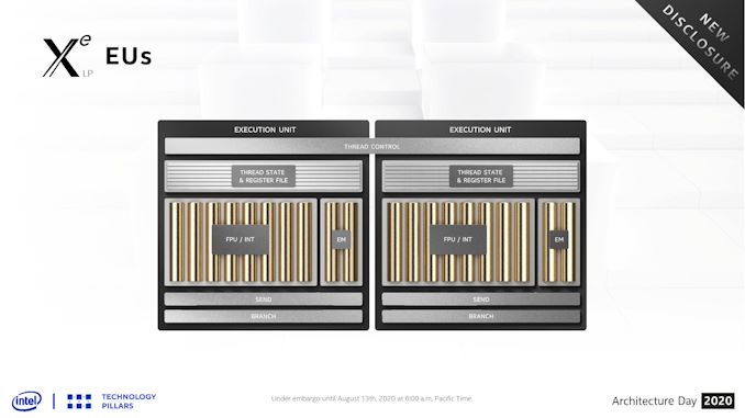
For Xe-LP, each of the 96 execution units have 10 ALUs, and they are split differently: the first 8 are for FP/INT, and the last 2 are for extended math. The 8 FP/INT in the new graphics support both INT16 (at double rate) and INT32 data types as well as new DP4a instructions can accelerate INT8 inference workloads. The new execution units also now work in pairs – two EUs will share a single thread control block to help assist with coordinated workload dispatch.
The graphics has its own L3 cache as well, which has a junction on the ring interconnect used inside Tiger Lake. In order to help accelerate graphics workloads further, Intel has doubled the bandwidth of the ring interconnect by essentially giving the SoC two rings, supporting 2x32B/cycle transfers bidirectionally.
Overall Intel is claiming up to 2x graphics throughput with the new Xe-LP compared to previous Gen11. Moving from 64 EUs to 96 EUs would immediately give +50% performance, and then the increase from 1100 MHz to 1450 MHz is another 32%. Together they would account for a 98% throughput increase, all other things scaling equally (memory bandwidth and such).
Tiger Lake: Media and Display
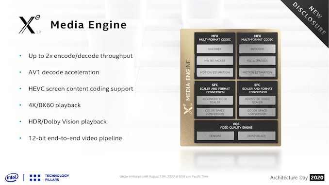
Tiger Lake will be Intel’s first official support for the AV1 codec in decode mode, and Intel has also doubled its encode/decode throughput for other popular codecs. This means a full hardware-based 12-bit video pipeline for HDR and 8K60 playback support.
Display Support for Tiger Lake is also extended with four 4K display pipelines. Connections over DP1.4, HDMI 2.0, Thunderbolt 4, and USB4 Type-C simultaneously is how Intel expects users to operate if all four outputs are needed at once. The display engine also supports HDR10, 12-bit BT2020 color, Adaptive Sync, and support for monitors up to 360 Hz.
Other SoC Adjustments
There are a few other elements about Tiger Lake that are known at an SoC level that should also be noted.
Tiger Lake now has support for LPDDR4X-4266 (32 GB max) as well as DDR4-3200 (64 GB max), which is a slight improvement over the previous generation Ice Lake on the LPDDR4X side. The silicon is also designed to support LPDDR5-5400, however we are unlikely to see any devices with LPDDR5 until the new year due to the extra validation requirements and the current extra cost that LPDDR5 brings. Intel discussed with its partners, and they preferred that Intel prioritized LPDDR4X validation to begin with. We have been told by Intel that LPDDR5 support on the current silicon, pending full validation, does not require a new silicon stepping.
Also related to memory, the new silicon now supports Total Memory Encryption. TME has been a popular feature of new silicon designs of late, and enables mobile device users to have the data held in the memory on a system physically secure against hardware attacks. In other systems we’ve been told that a feature like TME, when implemented correctly, only gives a 1-2% performance hit in the most usual worst case – Intel has not provided equivalent numbers as of yet. Given the type of feature this is, we suspect TME might be more of a vPro-enabled product feature, however we will have to get clarity on that.
One question that everyone likes to ask is die size. We took out some calipers and measured 13.49 x 10.70 mm = 144.34 mm2. This is rather close to our estimate from CES from the wafer photographs, where we guessed 146.10 mm2 (~1.2% error).
| Die Sizes | ||||||
| AnandTech | x | y | Die Size | Process | Cores | EUs/ CUs |
| AMD Zen 2 Chiplet | 10.32 | 7.34 | 75.75 mm2 | TSMC N7 | 8 | - |
| Intel Ice Lake | 11.44 | 10.71 | 122.52 mm2 | Intel 10 | 4 | 64 |
| Intel Tiger Lake | 13.49 | 10.70 | 144.34 mm2 | Intel 10SF | 4 | 96 |
| AMD Picasso | 19.21 | 10.92 | 209.78 mm2 | GF 12 | 4 | 11 |
| AMD Renoir APU | 13.59 | 10.98 | 149.22 mm2 | TSMC N7 | 8 | 8 |
There are also security features, which we will cover in the next page.
New Instructions and Updated Security
When a new generation of processors is launched, alongside the physical design and layout changes made, this is usually the opportunity to also optimize instruction flow, increase throughput, and enhance security.
Core Instructions
When Intel first stated to us in our briefings that by-and-large, aside from the caches, the new core was identical to the previous generation, we were somewhat confused. Normally we see something like a common math function get sped up in the ALUs, but no – the only additional changes made were for security.
As part of our normal benchmark tests, we do a full instruction sweep, covering throughput and latency for all (known) supported instructions inside each of the major x86 extensions. We did find some minor enhancements within Willow Cove.
- CLD/STD - Clearing and setting the data direction flag - Latency is reduced from 5 to 4 clocks
- REP STOS* - Repeated String Stores - Increased throughput from 53 to 62 bytes per clock
- CMPXCHG16B - compare and exchange bytes - latency reduced from 17 clocks to 16 clocks
- LFENCE - serializes load instructions - throughput up from 5/cycle to 8/cycle
There were two regressions:
- REP MOVS* - Repeated Data String Moves - Decreased throughput from 101 to 93 bytes per clock
- SHA256MSG1 - SHA256 message scheduling - throughput down from 5/cycle to 4/cycle
It is worth noting that Willow Cove, while supporting SHA instructions, does not have any form of hardware-based SHA acceleration. By comparison, Intel’s lower-power Tremont Atom core does have SHA acceleration, as does AMD’s Zen 2 cores, and even VIA’s cores and VIA’s Zhaoxin joint venture cores. I’ve asked Intel exactly why the Cove cores don’t have hardware-based SHA acceleration (either due to current performance being sufficient, or timing, or power, or die area), but have yet to receive an answer.
From a pure x86 instruction performance standpoint, Intel is correct in that there aren’t many changes here. By comparison, the jump from Skylake to Cannon Lake was bigger than this.
Security and CET
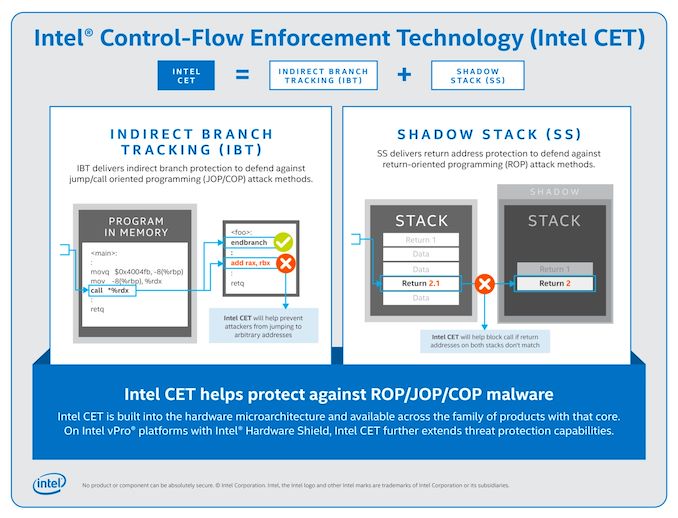
On the security side, Willow Cove will now enable Control-Flow Enforcement Technology (CET) to protect against a new type of attack. In this attack, the methodology takes advantage of control transfer instructions, such as returns, calls and jumps, to divert the instruction stream to undesired code.
CET is the combination of two technologies: Shadow Stacks (SS) and Indirect Branch Tracking (IBT).
For returns, the Shadow Stack creates a second stack elsewhere in memory, through the use of a shadow stack pointer register, with a list of return addresses with page tracking - if the return address on the stack is called and not matched with the return address expected in the shadow stack, the attack will be caught. Shadow stacks are implemented without code changes, however additional management in the event of an attack will need to be programmed for.
New instructions are added for shadow stack page management:
- INCSSP: increment shadow stack pointer (i.e. to unwind shadow stack)
- RDSSP: read shadow stack pointer into general purpose register
- SAVEPREVSSP/RSTORSSP: save/restore shadow stack (i.e. thread switching)
- WRSS: Write to Shadow Stack
- WRUSS: Write to User Shadow Stack
- SETSSBSY: Set Shadow Stack Busy Flag to 1
- CLRSSBSY: Clear Shadow Stack Busy Flag to 0
Indirect Branch Tracking is added to defend against equivalent misdirected jump/call targets, but requires software to be built with new instructions:
- ENDBR32/ENDBR64: Terminate an indirect branch in 32-bit/64-bit mode
Full details about Intel’s CET can be found in Intel’s CET Specification.
At the time of presentation, we were under the impression that CET would be available for all of Intel’s processors. However we have since learned that Intel’s CET will require a vPro enabled processor as well as operating system support for Hardware-Enforced Stack Protection. This is currently available on Windows 10’s Insider Previews. I am unsure about Linux support at this time.
Update: Intel has reached out to say that their text implying that CET was vPro only was badly worded. What it was meant to say was 'All CPUs support CET, however vPro also provides additional security such as Intel Hardware Shield'.
AI Acceleration: AVX-512, Xe-LP, and GNA2.0
One of the big changes for Ice Lake last time around was the inclusion of an AVX-512 on every core, which enabled vector acceleration for a variety of code paths. Tiger Lake retains Intel’s AVX-512 instruction unit, with support for the VNNI instructions introduced with Ice Lake.
It is easy to argue that since AVX-512 has been around for a number of years, particularly in the server space, we haven’t yet seen it propagate into the consumer ecosphere in any large way – most efforts for AVX-512 have been primarily by software companies in close collaboration with Intel, taking advantage of Intel’s own vector gurus and ninja programmers. Out of the 19-20 or so software tools that Intel likes to promote as being AI accelerated, only a handful focus on the AVX-512 unit, and some of those tools are within the same software title (e.g. Adobe CC).
There has been a famous ruckus recently with the Linux creator Linus Torvalds suggesting that ‘AVX-512 should die a painful death’, citing that AVX-512, due to the compute density it provides, reduces the frequency of the core as well as removes die area and power budget from the rest of the processor that could be spent on better things. Intel stands by its decision to migrate AVX-512 across to its mobile processors, stating that its key customers are accustomed to seeing instructions supported across its processor portfolio from Server to Mobile. Intel implied that AVX-512 has been a win in its HPC business, but it will take time for the consumer platform to leverage the benefits. Some of the biggest uses so far for consumer AVX-512 acceleration have been for specific functions in Adobe Creative Cloud, or AI image upscaling with Topaz.
Intel has enabled new AI instruction functionality in Tiger Lake, such as DP4a, which is an Xe-LP addition. Tiger Lake also sports an updated Gaussian Neural Accelerator 2.0, which Intel states can offer 1 Giga-OP of inference within one milliwatt of power – up to 38 Giga-Ops at 38 mW. The GNA is mostly used for natural language processing, or wake words. In order to enable AI acceleration through the AVX-512 units, the Xe-LP graphics, and the GNA, Tiger Lake supports Intel’s latest DL Boost package and the upcoming OneAPI toolkit.
Section by Andrei Frumusanu
Cache Architecture: The Effect of Increasing L2 and L3
Although the Willow Cove core doesn’t bring all that many improvements on the actual core microarchitecture, one big update for the design is the new memory subsystem thanks to a quite significant change in the caches of the design.
Intel here has made some big changes in the L2 caches as well as the L3 cache slices: they’ve both grown considerably bigger and have had their cache line exclusivity altered.
| Core Cache Comparison | ||||||
| Willow Cove |
AnandTech | Sunny Cove |
Cannon Lake |
Skylake | AMD Zen 2 |
|
| 48 KB 12-way |
L1-D | 48 KB 12-way |
32 KB 8-way |
32 KB 8-way |
32 KB 8-way |
|
| 32 KB 8-way |
L1-I | 32 KB 8-way |
32 KB 8-way |
32 KB 8-way |
32 KB 8-way |
|
| 1280 KB 20-way |
L2 | 512 KB 8-way |
256 KB 4-way |
256 KB 4-way |
512 KB 8-way |
|
| 3 MB (<=12MB) 12-way |
L3/core (Max. Total) |
2 MB (<=8MB) 16-way |
2 MB (<=8MB) 16-way |
2 MB (<=20MB) 16-way |
4 MB (<=16MB) 16-way |
|
| 2304 | uOp Cache | 2304 | 1536 | 1536 | 4096 | |
The L1-D and L1-I caches on Willow Cove remain the same as the predecessor Sunny Cove design, which means they retain their 48KB 12-way associative designs for the data cache, respectively 32KB 8-way associative design for the instruction cache.
Where things differ significantly is in the L2. This time around Intel has completely redesigned this part of the core and has increased the capacity by 150% by increasing it from 512KB to 1280KB. Furthermore, the actual usable capacity has increased even more between generations as the new design now moves from being inclusive of the L1 caches, to a non-inclusive design.
Compromises that had been made when increasing the cache by this great of an amount is in the associativity, which now increases from 8-way to a 20-way, which likely decreases conflict misses for the structure.
On the L3 side, there’s also been a change in the microarchitecture as the cache slice size per core now increases from 2MB to 3MB, totalling to 12MB for a 4-core Tiger Lake design. Here Intel actually reduced the associativity from 16-way to 12-way, likely increasing cache line conflict misses and decreasing access parallelism.
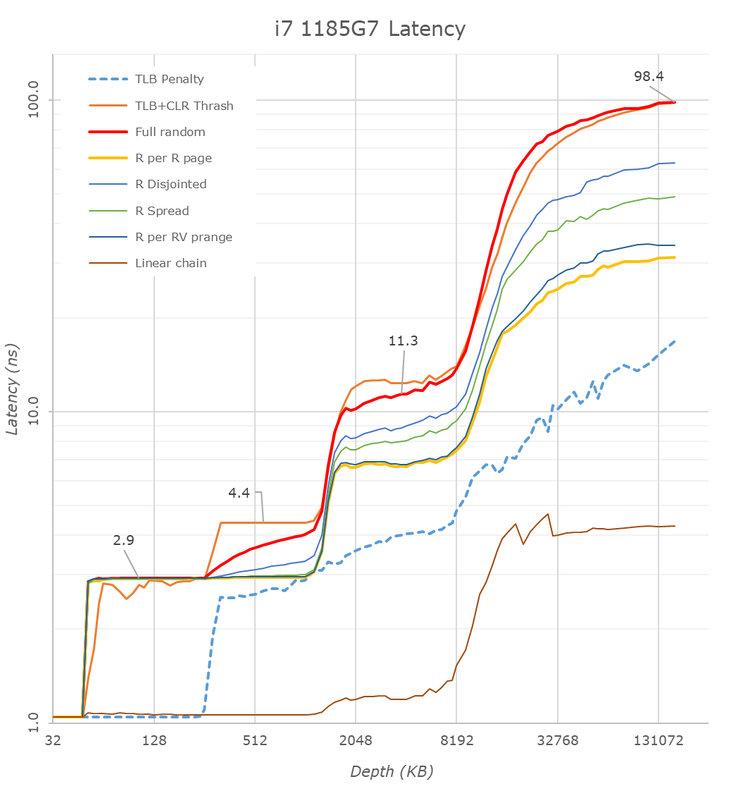
When looking at the i7-1185G7 in our custom latency test tool, we immediately note the cache structure changes when comparing the results to a previous generation design such as the Ice Lake based i7-1065G7.
First thing to note here about the results is the frequency of the cores as well as the system’s DRAM configurations: The Tiger Lake part clocked up to 4800MHz and featured LPDDR4X-4266 with 36-39-39 timings, while the Ice Lake figures were measured on a Surface Laptop 3, clocking at 3900MHz and LPDDR4X-3733 32-34-34.
On the L1 side of things as expected we don’t see much changes in latency beyond the clock frequency increase which brings access times down from 1.3ns to 1.04ns.
Moving onto the L2 cache is where things become interesting. Absolute access time figures go down from 3.3 to 2.9ns, but the Willow Cove core now extends this access time across a deeper depth up to 1.25MB – exactly as we’d expect given the cache’s larger structure this generation.
The access latencies don’t extend exactly to 12MB because starting from 8MB we’re exceeding the coverage of the L2 TLB at which point the core has to page-walk, incurring heavier latency penalties.
Intel hasn’t changed the TLBs this generation, still maintaining a 64-page L1 TLB which means that starting from 256KB depth (at 4KB pages), we’re seeing an increase in access times for access patterns which miss the first level TLB.
On the L3 we’re getting some interesting results which are both positive and negative. The positive thing of course is the vastly increased depth of the cache which now sees extended good access latencies up around the 10-12MB mark. What’s seemingly not so great is the fact that the absolute latency figures here aren’t really any different to Ice Lake, ending up nearly identical even though the Tiger Lake design clocks up to 23% higher in frequency. This is a sign that the cycle-access latencies of the design have gone up quite a bit this generation.
On deeper depths reaching DRAM, things are massively improved for the new Tiger Lake design: Full random access at an equal 160MB depth here in the graphs improve from 130ns to 98ns. Admittedly, we’re using different DRAM configurations between the two test platforms and the Tiger Lake system is using 14% higher clocked memory, but it does have worse timings. The actual latency improvements are well beyond the theoretical DRAM access latency difference, so what I think is happening here is that Intel has made some improvements to their memory subsystem and memory controllers.
We’re seeing a slight change in the access pattern latencies compared to Ice Lake, especially in the “R per R page” pattern which remains within a single memory page before moving onto the next, with the access latencies being 30% better than on Ice Lake. This does point out to some actual structural changes on the memory controller side, as otherwise the prefetcher behaviour at least doesn’t see any changes at all- with things being pretty much similar to back to what we’ve seen on Skylake.
What’s also interesting for the new design is that straightforward linear streaming patterns have seen a slight degradation, increasing from 3.516ns to 4.277ns on the new core. This is likely a side-effect of the added cache cycles in the lower level caches of the new Willow Cove core.
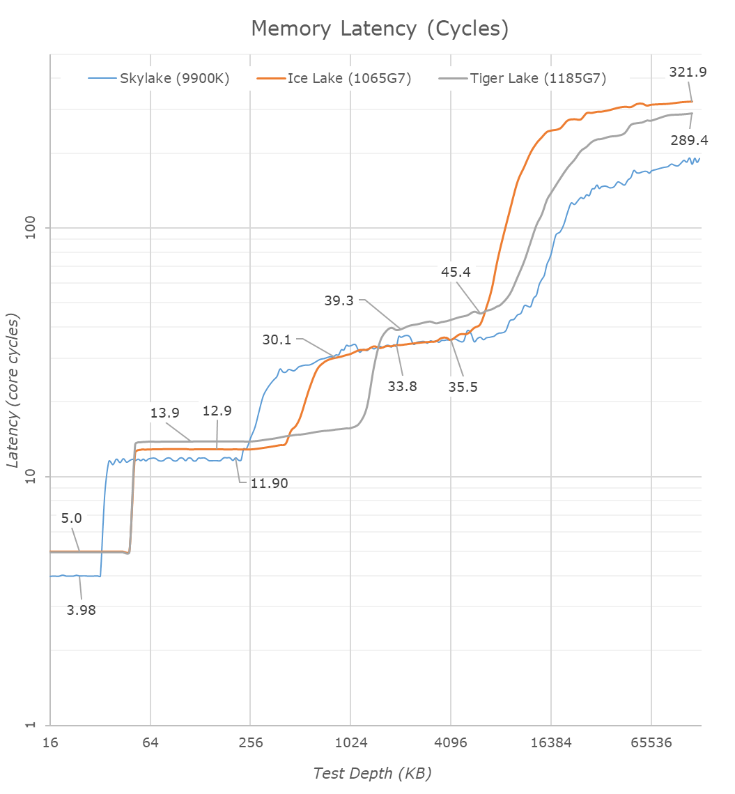
Translating the latency graph from nanoseconds to core cycles, we’re seeing the generational structural changes between the Sunny Cove and Willow Cove designs.
| Core Cache Latency (in core cycles) | ||||||
| Willow Cove | AnandTech | Sunny Cove | Cannon Lake |
Skylake | AMD Zen 2 |
|
| 5 | L1 | 5 | 4 | 4 | 4 | |
| 14 | L2 | 13 | 12 | ~12 | 12 | |
| 39-45 | L3 | 30-36 | 26-37 | 34 | ||
The L1D cache remains the same at 5 cycles latency, which is still a 1-cycle degradation over Skylake cores.
The L2 seemingly has gone up from 13 cycles to 14 cycles in Willow Cove, which isn’t all that bad considering it is now 2.5x larger, and its associativity has gone up. It’s interesting to contrast this against other similarly sized caches in the industry: Arm’s Neoverse N1 core has a 1MB cache coming in at 11-cycle latency, whilst their new X1 core shaves this down to 10 cycles. Of course, Intel’s designs clocks much higher, but the competitor’s design still would end up with better absolute access times.
The L3 cache cycle latency is a bit disappointing as we’re seeing essentially a +9 cycle degradation over the older design. This explains the previous access latencies which essentially just remained the same even though the core clocks in 23% higher.
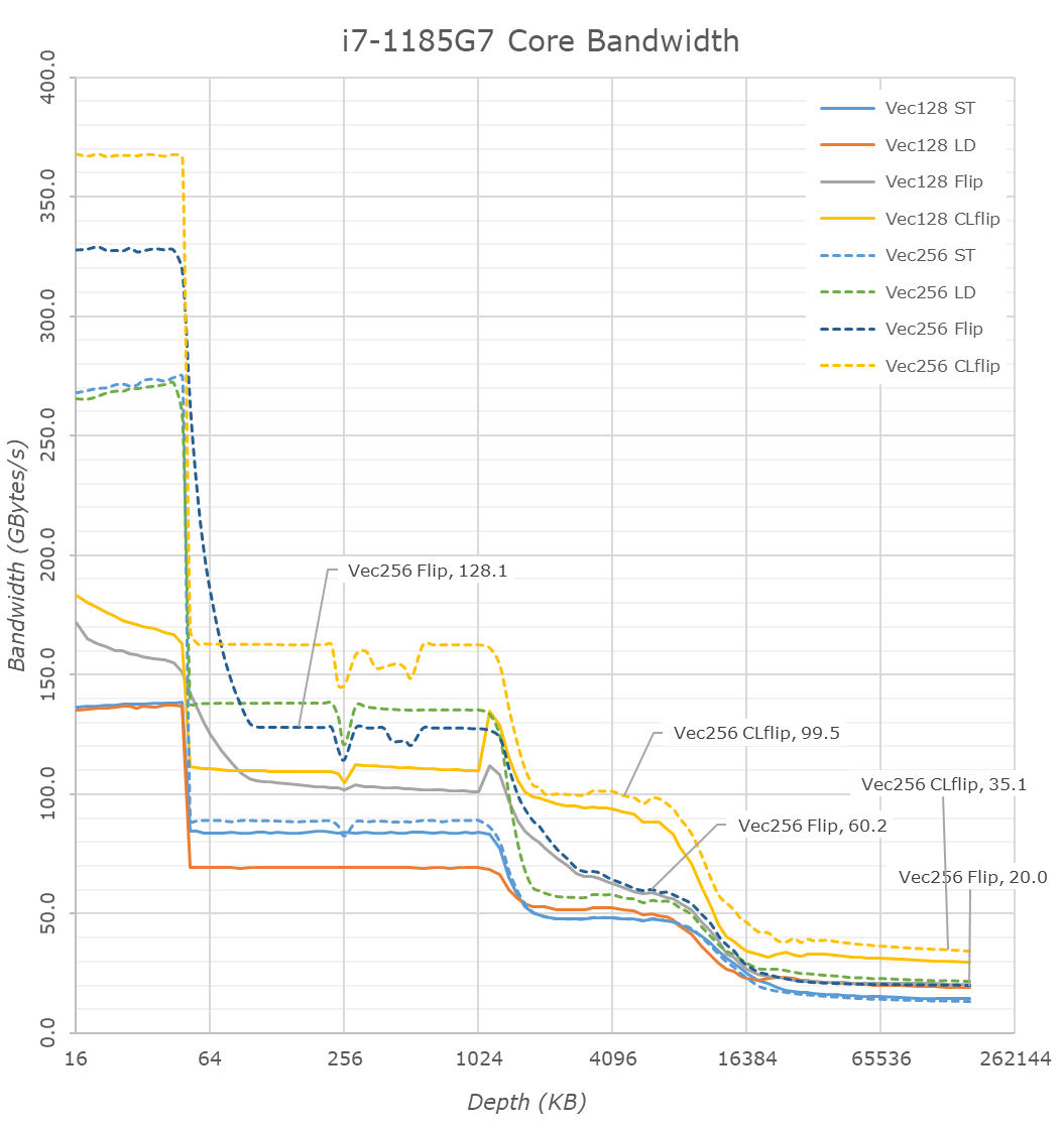
Finally, having a quick glance at the single-core bandwidth figures we’re looking if there’s been any significant structural changes in this aspect of the design.
On the L1 side of things, things are a bit odd as the figures don’t scale up as expected with the clock frequency, pure load and store bandwidth are indeed higher but the memory copy patterns are less than expected. In the L2 and L3 regions we can clearly see the increased depth of the caches. The L2 scales well with a near 19% increase in bandwidth which is in line with the clock uptick.
The L3 doesn’t scale that well as memory copies between cache lines here are only 5% faster than on Ice Lake, likely due to the increased access latencies of the caches.
In the DRAM region we’re actually seeing a large change in behaviour of the new microarchitecture, with vastly improved load bandwidth from a single core, increasing from 14.8GB/S to 21GB/s. Pure store bandwidth slightly goes down from 14.8GB/s to 13.5GB/s but that’s not quite important as a metric for x86 as the core first has to read out the memory before writing to it, as opposed to some of the non-temporal write optimisations we’ve seen from Arm processors.
More importantly, memory copies between cache lines and memory read-writes within a cache line have respectively improved from 14.8GB/s and 28GB/s to 20GB/s and 34.5GB/s. That’s a 35% improvement in copy bandwidth which is quite significant.
Overall, the new Willow Cove cores and the Tiger Lake memory subsystem seems sort of a mixed bag. The increased cache sizes are certainly welcome for workloads that have a larger memory-footprint; however, Intel’s L3 cache changes seem to have come with some larger compromises when it comes to latency. On the positive side, DRAM access latencies and bandwidth seem to have been drastically improved in the new design, and here it seems Intel made some good improvements in the fabric as well as the memory controllers of Tiger Lake.
Intel’s TDP Shenanigans Hurts Everyone
Every time we come round to talking about laptop power consumption on a new generation of Intel processors, we find that the goalposts have moved. The physics of power consumption and cooling are always the same (in this universe), however we find that the marketing focal point of Intel’s power consumption has shifted yet again, causing more confusion than I believe is warranted. Tiger Lake, in this case, is no exception.
For Tiger Lake, Intel is offering two sets of processors, as with previous generations. These used to be called the U-series, based at 15 watts, and the Y-series, at 4.5/7/9 watts, however for Tiger Lake the U and Y designations will no longer be used. This time users will have to fully understand Intel’s product SKU list in order to make sense of it. Good luck, Grandma.
What used to be called the U-series is now, from the perspective of engineering rather than marketing, known as the ‘UP3’ product packaging. These UP3 processors are identifiable in two ways: first, the processor name has a ‘5’ before the G, such as Core i7-1185G7; second, by the TDP range of 12-28 watts.
This time around Intel is not giving the historic U-series a fixed TDP value, but instead giving it a range of values, stating that ‘TDP is a poor metric’ for the type of systems these chips go into. Despite this statement, in the next breath Intel goes ahead and quotes the base frequency of the UP3 processors as the peak 28 W value.
For anyone untrained in reading Intel product names, one might easily be mistaken when comparing the previous generation Ice Lake to the new Tiger Lake parts. Suddenly the typical ‘U-Series’ 15 W processor, such as the Core i7-1065G7, was at 1.3 GHz, but is now replaced by the Core i7-1185G7, with a base frequency of 3.0 GHz. The names are so similar, and there’s only a one generation gap, so wow, that’s an amazing jump in one generation! Right? Right??
To make matters worse, the values for the 28 W base frequency are hard-coded into the processor string in the products. For anyone looking at the CPUID for one of these processors, that 28 W value is what they are going to see, even if the product is a fanless notebook running at 12 W. To give some credit, Intel in its online database also provides the base frequency at the lowest TDP value as well. But this is not hard-coded into the processor string like the 28 W value is.
One might forgive Intel if they also provide the 15 W value for these new processors in the online database. This would allow enthusiasts and key influencers to understand the product portfolio in an apples-to-apples comparison over the previous generation in this U-series bracket. However, this is not provided. It was not until I had obtained my review sample, found the value myself, and then returned the sample that Intel gave me this value for the single processor I had tested. This is how far the company seemingly wants to go to ‘remove’ this concept of TDP and power consumption.
So what do we get if we look at Intel’s own processor database?
- Base Frequency at the lowest PL1 value
- Base Frequency at the highest PL1 value
- Maximum Turbo Frequency at a not-given PL2 value
The metrics that Intel leaves out include:
- The base frequency at the U-series 15 W value (for UP3)
- The PL2 value for which the maximum turbo frequency is defined
- The number of cores that the maximum turbo frequency is valid
- The turbo frequency when all cores are loaded
Intel does sometimes, when products are launched, provide that final value of an all-core turbo. However users will have to be looking at coverage in places like AnandTech at the time, as it is not on the product page at Intel.
The other three values listed as not given are not provided to us, even when requested, with the common response being ‘these values are proprietary’. This is despite the fact that most of these values can be easily discovered by having the hardware at hand and probing the relevant output. It is unlikely that one outlet will have one of each processor to discover this data and provide a table, and even then that only matters if a user can find it, as it is not on Intel’s website. From my point of view, and I’ve told Intel this countless times, it would offer a more complete picture (and a better marketing message that Intel cares for its enthusiast audience that cares about this) if the data was provided in full.
If that mish-mash of data didn’t confuse you, how is this for completeness. Intel also announced the Y-series equivalent processors, which have UP4 style of packaging. Intel listed these products as having a TDP range of 7 watts to 15 watts, and the online database has the base frequency of these values. But in the product launch specification tables, to add insult to injury, Intel provided the base frequency for these processors at 9 watts, allowing for an apples-to-apples comparison. Go figure. It can be understandable when there’s some inconsistency in detail between products from different business units under the same company, however these two client processor groups couldn’t be closer together, given they’re cited in the same table on the same slide of the same presentation.
(Sometimes things like this are caught during press pre-briefs and fixed for the public announcement, however Intel decided not to pre-brief any press this time around.)
A Recap on TDP, PL1, PL2
For any new readers, that previous section can sound very complex. Power consumption, at a high level, should be a very simple thing to discuss. Power goes in, then power goes out - it used to be as simple as this. However to extract the most performance out of the hardware, as well as focusing performance in areas where it is more vital (such as turbo), has made it complex. Discussing elements like power draw and thermal design points has been an iterative process over the last decade. For those who haven’t delved into the topic before, here’s a short summary, mostly with respect to Intel.
Intel’s definition of TDP, or the thermal design point, does not mean the peak power draw of the processor as it does with some of the competition.
The thermal design point of an Intel processor is a measure of the expected cooling required for that processor for it to perform within normal operation at its base frequency with a high load. The TDP has the units of watts, for the amount of joules of energy per second that needs to be removed from the system to maintain normal operation.
Because TDP is in watts, the TDP is often equated as the power draw of that processor. This simplification is, for our purposes, a valid identity to make, as we’re dealing with the cooling a processor needs.
With that in mind, Intel defines the TDP as the power draw of a processor at a guaranteed minimum frequency with a sustained highly demanding workload within a suitable environment. What that means is that if you have a compute heavy workload (like rendering) and as long as your system isn’t somewhere abnormal (such as in an oven or at the north/south pole), the processor will not go above the TDP value for power consumption as well as offer the minimum frequency stated with that power - if it does not, Intel will honor its warranty and replace it.
Normally we refer to Intel’s TDP rating as the ‘sustained power draw’ for the given base frequency. It is sometimes referred to as the ‘power level 1’ or PL1 of that processor. So, for example, the Tiger Lake processor we are testing today supports a range of TDP values, such as 12 W, with a given minimum frequency, in this case 1200 MHz at 12 W. Because Tiger Lake offers a range of TDP values, it can get complicated - we will cover this in a bit.
Alongside the PL1 value, these processors also have a PL2 value. This is commonly referred to as the peak power consumption while the processor is running in a turbo performance mode, and the value of PL2 is higher than PL1. Intel rarely quotes an official value for PL2 when announcing a product, but it always announces the frequency associated with PL2, which is a maximum turbo frequency. Because the turbo mode is a limited time mode, these frequencies are reached during user-experience events, such as touching a screen, loading software, or even on key presses. In between these user-experience events, the system often moves out of the turbo mode to save power, and it can do so within 1/60th of a second.
The frequency associated with this PL2 is thus a limited time frequency, rather than a sustained frequency, and can also be limited by how many cores it can apply to at any one time. This is also the frequency that is listed on the box or laptop, alongside the PL1 value, which some users feel is not a genuine reflection of sustained performance.
PL2 is also used in the initial phase of a high-performance workload. Aside from thermal considerations, Intel also has a metric called Tau, in seconds, which is a measure of how long the PL2 turbo mode can be sustained for a ‘typical high performance’ workload. Thus if a PL2 is rated at 50 W, with a Tau of 10 seconds, then the ‘turbo budget’ is 500 joules of energy. If the workload is more strenuous than Intel’s metric, then the actual time for turbo may be shorter as that 500 joules budget is used. The budget is replenished if less than PL1 is needed (the actual calculation is more complex, based on an exponential weighted average time window, but has the same principle).
To summarize:
- PL1, or TDP, is the sustained power draw for a given minimum frequency
- PL2, or turbo, is the peak power draw for a maximum frequency under a turbo mode
- A turbo mode can either be a user-experience event, or the initial phase of a high-performance workload
- Tau is a time measure for how long PL2 can be sustained in a high-performance workload
- Tau is based on a typical high-performance workload defined by Intel
As noted before, the PL1 of a processor can be a range of values. When the processor goes into a product however, it is set to a fixed value in that range. This value is often determined by the type of product (thin and light notebook, vs gaming notebook, for example).
Beyond this, Intel notes that its suggested values for PL2 and Tau are only recommendations. Laptop manufacturers are free to choose whatever values for PL2 and Tau they believe are sufficient for the system they are building. As we have seen in some fanless designs, PL2 and Tau can be incredibly small, whereas in a desktop, Tau could be effectively infinite.
Tiger Lake Metrics
How does this play into Tiger Lake? For this review, we have the Core i7-1185G7. Intel gives us the following values on its online database:
- At 12 W TDP, the Base Frequency guaranteed is 1200 MHz
- At 28 W TDP, the Base Frequency guaranteed is 3000 MHz
- In a turbo mode, the peak frequency will be 4800 MHz.
A few more details were given at the time the processor was launched:
- The peak frequency of 4800 MHz is valid only when one core is loaded
- The peak frequency is 4300 MHz when more than one core is loaded
- The maximum power draw in the turbo mode is ~50 W*
*It should be noted that the last figure was not given directly, but through analysis of power consumption data provided in the slide deck accompanying in the launch. The value of 50 W is valid regardless of what TDP mode is in play.
From testing the Core i7-1185G7 we have, we can also provide the following data point:
- At 15 W TDP the Base Frequency guaranteed is 1800 MHz
Unfortunately we have no insight into the other UP3 Tiger Lake processors.
Comparing Power Consumption: TGL to TGL
On the first page of this review, I covered that our Tiger Lake Reference Design offered three different power modes so that Intel’s customers could get an idea of performance they could expect to see if they built for the different sustained TDP options. The three modes offered to us were:
- 15 W TDP (Base 1.8 GHz), no Adaptix
- 28 W TDP (Base 3.0 GHz), no Adaptix
- 28 W TDP (Base 3.0 GHz), Adaptix Enabled
Intel’s Adaptix is a suite of technologies that includes Dynamic Tuning 2.0, which implements DVFS feedback loops on top of supposedly AI-trained algorithms to help the system deliver power to the parts of the processor that need it most, such as CPU, GPU, interconnect, or accelerators. In reality, what we mostly see is that it reduces frequency in line with memory access stalls, keeping utilization high but reducing power, prolonging turbo modes.
Compute Workload
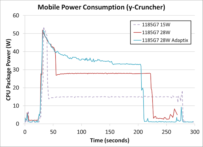
When we put these three modes onto a workload with a mix of heavy AVX-512 compute and memory accesses, the following is observed.
Note that due to time constraints this is the only test we ran with Adaptix enabled.
This is a fixed workload to calculate 2.5 billion digits of Pi, which takes around 170-250 seconds, and uses both AVX-512 and 11.2 GB of DRAM to execute. We can already draw conclusions.
In all three power modes, the turbo mode power limit (PL2) is approximately the same at around 52 watts. As the system continues with turbo mode, the power consumed is decreased until the power budget is used up, and the 28 W mode has just over double the power budget of the 15 W mode.
Adaptix clearly works best like this, and although it initially follows the same downward trend as the regular 28 W mode, it levels out without hitting much of a ‘base’ frequency at all. Around about the 150 second mark (120 seconds into the test), there is a big enough drop followed by a flat-line which would probably indicate a thermally-derived sustained power mode, which occurs at 33 watts.
The overall time to complete this test was:
- Core i7-1185G7 at 15 W: 243 seconds
- Core i7-1185G7 at 28 W: 191 seconds
- Core i7-1185G7 at 28 W Adaptix: 174 seconds
In this case moving from 15 W to 28 W gives a 27% speed-up, while Adaptix is a total 40% speed-up.
However, this extra speed does come at the cost of total power consumed. With most processors, the peak efficiency point is when the system is at idle, and while these processors do have a good range of high efficiency, when the peak frequencies are requested then we are in a worst case scenario. Because this benchmark measures power over time, we can integrate to get total benchmark power consumed:
- Core i7-1185G7 at 15 W: 4082 joules
- Core i7-1185G7 at 28 W: 6158 joules
- Core i7-1185G7 at 28 W Adaptix: 6718 joules
This means that for the extra 27% performance, an extra 51% power is used. For Adaptix, that 40% extra performance means 65% more power. This is the trade off with the faster processors, and this is why battery management in mobile systems is so important - if a task is lower priority and can be run in the background, then that is the best way to do it to conserve battery power. This means things like email retrieval, or server synchronization, or thumbnail generation. However, because users demand the start menu to pop up IMMEDIATELY, then user-experience events are always put to the max and then the system goes quickly to idle.
Professional ISV Workload
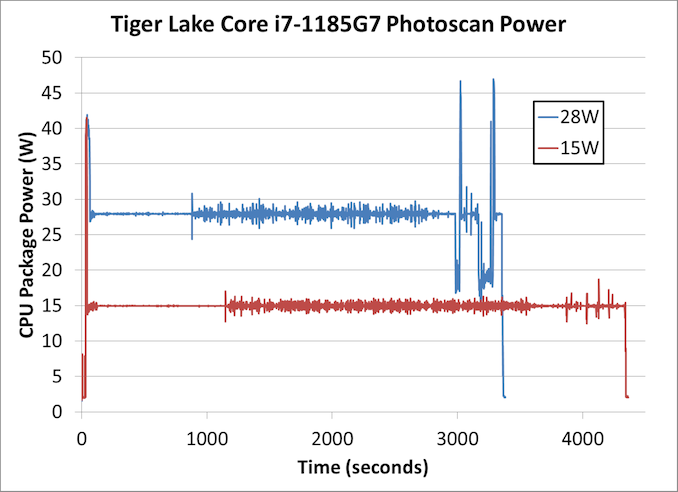
In our second test, we put our power monitoring tools on Agisoft’s Photoscan. This test is somewhat of a compute test, split into four algorithms, however some sections are more scalable than others. Normally in this test we would see some sections rely on single threaded performance, while other sections use AVX2.
This is a longer test, and so the immediate turbo is less of a leading factor across the whole benchmark. For the first section the system seems content to sit at the respective TDPs, but the second section shows a more variable up and down as power budget is momentarily gained and then used up immediately.
Doing the same maths as before,
- At 15 W, the benchmark took 4311 seconds and consumed 64854 joules
- At 28 W, the benchmark took 3330 seconds and consumed 92508 joules
For a benchmark that takes about an hour, a +30% performance uplift is quite considerable, however it comes at the expense of +43% power. This is a better ratio than the first compute workload, but still showcases that 28 W is further away from Tiger Lake’s ideal efficiency point.
Note that the power-over-time graph we get for Agisoft on a mobile processor looks very different to that of a desktop processor, as a mobile processor core can go above the TDP budget with fewer threads.
This leads to the dichotomy of mobile use cases with respect to the marketing that goes on for these products - as part of the Tiger Lake launch, Intel was promoting its use for streaming, professional workflows such as Adobe, video editing and content creation, and AI acceleration. All of these are high-performance workloads, compared to web browsing or basic office work. Partly because Tiger Lake is built on the latest process technology, as well as offering Intel’s best performing CPU and GPU cores, the product is going to be pitched in the premium device market for the professionals and prosumers that can take advantage.
Comparing 15 W TGL to 15 W ICL to 15 W Renoir
Despite the hullaballoo with the 28 W numbers on Tiger Lake, we suspect that most OEMs will still be positioning the hardware inside chassis built for the 15 W ultraportable market. This is where most of Intel’s OEMs have had success over the last decade, as the lower cooling requirements allow for a more user-friendly design. At 28 W, there is more of a cross-over into laptops that have discrete graphics options, and the main company that has succeeded in offering 28 W laptops without discrete graphics has been Apple - most Intel partners, if they want discrete graphics, end up looking at the 45 W processors with more cores.
So in that respect, our main battle should occur between the products built for 15 W. To that end we have been able to put the three together that will command this holiday season’s offerings: Ice Lake, Tiger Lake, and AMD’s Renoir.
- For our Ice Lake system, we have the Microsoft Surface Laptop 3. This has the top-of-the-line quad-core Core i7-1065G7, along with 16 GB of LPDDR4X-3733. Base 1.3 GHz, Turbo 3.9 GHz. Because this is an OEM design, Microsoft have determined the PL1 and PL2 values, and so they might be different from a ‘base’ design, however this is data from a real system.
- The Tiger Lake system is our Reference Design from Intel, running the quad-core Core i7-1185G7 at 15 W TDP mode. It has 16 GB of LPDDR4X-4266. Base 1.8 GHz, Turbo 4.8 GHz.
- Our AMD Renoir system is one of the most premium examples of AMD’s Ryzen Mobile in a 15W form factor, the Lenovo Yoga Slim 7 with the eight-core Ryzen 7 4800U processor. Even when set to the highest performance mode, the system still operates with a 15 W sustained power draw. It comes equipped with 16 GB of LPDDR4X-4266. Base 1.8 GHz, Turbo 4.2 GHz.
Compute Workload
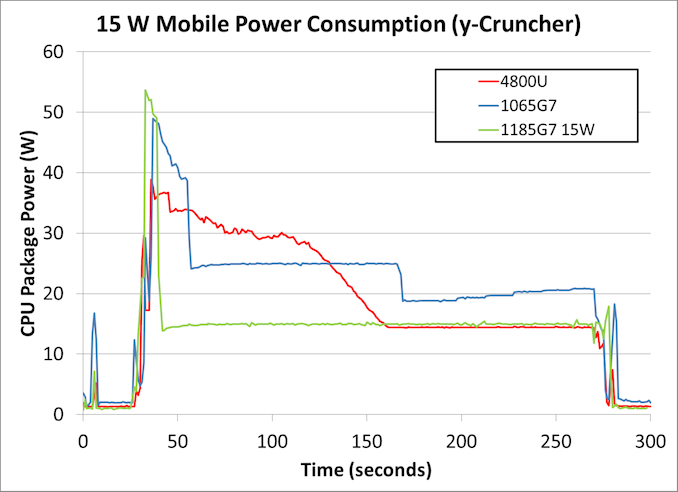
For our 15 W comparisons, we can look again at the same benchmarks as the previous page. First up is y-Cruncher, an AVX2/AVX512 compute workload that tasks the CPU and the memory by calculating 2.5 billion digits of Pi, and requires ~11 GB of DRAM.
As we saw on the previous page, our Tiger Lake system in green at 15 W turbos up to ~53 watts before very quickly coming down to 15 W for the rest of the test.
The Microsoft Surface Laptop 3, by virtue of an OEM system, has different behavior - it turbos for longer, settles into a short turbo limit of 25 W, and then after about two minutes comes down to 20 W. The system then appears to opportunistically up the power draw until the end of the test, likely due to detecting extra thermal headroom.
The AMD Renoir processor does not turbo as high, peaking at only 38.9 W. Over the course of the next 100 seconds or slow, we see a small ramp down to just under 30 watts, before a more consistent decline over 30 seconds to 15 W, before staying at 15 W for the full test. The Renoir here has eight cores rather that four, but is running AVX2 rather than AVX-512 code.
The results are as follows:
- Ice Lake: 233 seconds, for 6072 joules, averaging 26.1 W
- Tiger Lake: 241 seconds for 4082 joules, averaging 17.0 W
- Renoir: 234 seconds for 5386 joules, averaging 23.0 W
All three systems perform the test in roughly the same amount of time, however the Tiger Lake system is very much ahead for efficiency. Tiger Lake effectively shaves off a third of the power from the previous generation Ice Lake system. We weren’t expecting this much of a jump from Ice Lake to Tiger Lake, but it would appear that Intel has done some work on the AVX-512 unit, and is putting that new high-performance transistor to use.
Professional ISV Workload
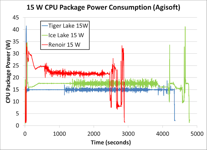
Moving onto the Agisoft test - as mentioned on the previous page, this is a 2D image to 3D modeling workflow where the algorithm comes in four stages, some of which prefer full multi-thread throughput, while others are more frequency and memory sensitive.
First, the Renoir finishes in almost half the time, mostly due to the fact that it has double the number of cores - there is no AVX-512 codepath in this test, and so all the processors rely on a mix of SSE, AVX, and perhaps some AVX2. That aside, the turbo behavior of Renoir is very interesting - we get almost 10 minutes of higher-than-base performance before the algorithm sets into a routine, hovering around 22 W. Because this test doesn’t attack the vector units as hard as the previous test, it may be a case that the Renoir system can manage the power distribution a bit better between the eight cores, allowing for the higher turbo.
Between the Ice Lake and the Tiger Lake, from the graph it would appear to be a double win for Tiger Lake, finishing in a shorter time but also consuming less power. The results are:
- 15 W Renoir: 2842 seconds for 62660 joules
- 15 W Ice Lake: 4733 seconds for 82344 joules
- 15 W Tiger Lake: 4311 seconds for 64854 joules
In this case, it’s a win for Renoir - a lot shorter time, and better power to boot, derived from the eight cores built on TSMC 7nm. Tiger Lake still represents a good jump over Ice Lake, offering 10% better performance at only 79% of the power, or a 13% increase in performance efficiency.
Section by Andrei Frumusanu
CPU ST Performance: SPEC 2006, SPEC 2017
SPEC2017 and SPEC2006 is a series of standardized tests used to probe the overall performance between different systems, different architectures, different microarchitectures, and setups. The code has to be compiled, and then the results can be submitted to an online database for comparison. It covers a range of integer and floating point workloads, and can be very optimized for each CPU, so it is important to check how the benchmarks are being compiled and run.
We run the tests in a harness built through Windows Subsystem for Linux, developed by our own Andrei Frumusanu. WSL has some odd quirks, with one test not running due to a WSL fixed stack size, but for like-for-like testing is good enough. SPEC2006 is deprecated in favor of 2017, but remains an interesting comparison point in our data. Because our scores aren’t official submissions, as per SPEC guidelines we have to declare them as internal estimates from our part.
For compilers, we use LLVM both for C/C++ and Fortan tests, and for Fortran we’re using the Flang compiler. The rationale of using LLVM over GCC is better cross-platform comparisons to platforms that have only have LLVM support and future articles where we’ll investigate this aspect more. We’re not considering closed-sourced compilers such as MSVC or ICC.
clang version 10.0.0

clang version 7.0.1 (ssh://[email protected]/flang-compiler/flang-driver.git

 24bd54da5c41af04838bbe7b68f830840d47fc03)
-Ofast -fomit-frame-pointer

-march=x86-64

-mtune=core-avx2

-mfma -mavx -mavx2
Our compiler flags are straightforward, with basic –Ofast and relevant ISA switches to allow for AVX2 instructions. We decided to build our SPEC binaries on AVX2, which puts a limit on Haswell as how old we can go before the testing will fall over. This also means we don’t have AVX512 binaries, primarily because in order to get the best performance, the AVX-512 intrinsic should be packed by a proper expert, as with our AVX-512 benchmark.
To note, the requirements for the SPEC licence state that any benchmark results from SPEC have to be labelled ‘estimated’ until they are verified on the SPEC website as a meaningful representation of the expected performance. This is most often done by the big companies and OEMs to showcase performance to customers, however is quite over the top for what we do as reviewers.
Starting off with our SPEC2006 analysis for Tiger Lake, given that we’re extremely familiar with the microarchitectural characteristics of these workloads:
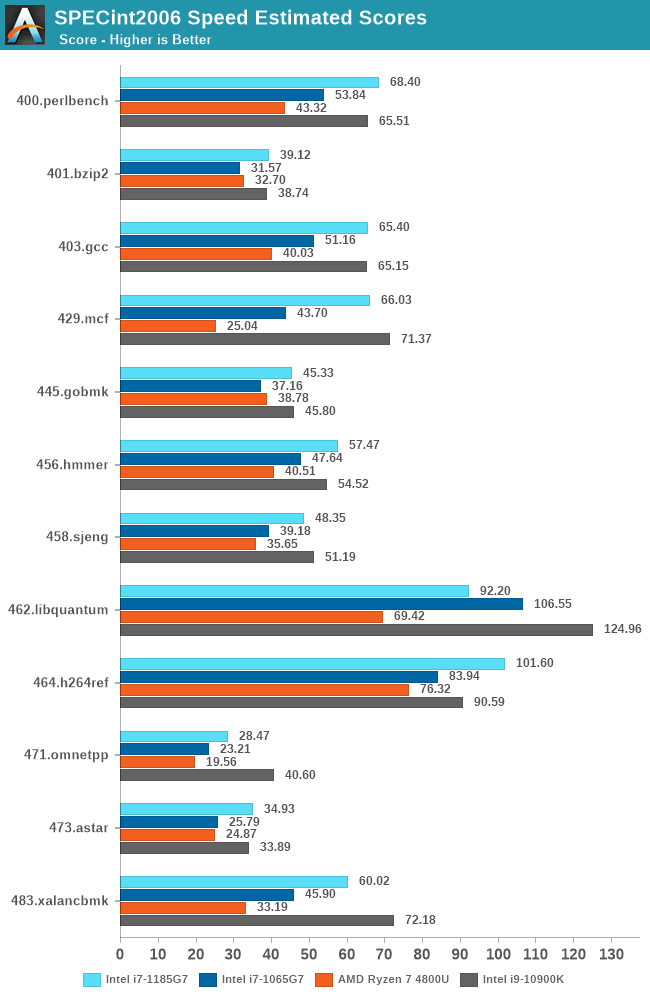
As a note, the Tiger Lake figures published in the detailed sub-scores represent the 28W TDP configuration option of the platform, with the core mostly clocking to 4800MHz and all other aspects the device allowing for maximum speed. This allows us for a pure microarchitectural analysis.
The generational improvements of the new Sunny Cove design here is showing very much its advertised characteristics of the microarchitecture.
Starting off with high-IPC and backend execution-bound workloads such as 456.hmmer we’re seeing a near linear performance increase with clock frequency. Sunny Cove here had larger IPC improvements but the Ice Lake design was rather limited in its clock frequency, most of the time still losing out to higher-clocked Skylake designs.
This time around with the major frequency boost, the Tiger Lake chip is able to even outperform the desktop i7-10900K at 5.3GHz as long as memory doesn’t become a bottleneck.
IPC/performance-per-clock wise, things are mostly flat between generation at +-2% depending on workloads, but 473.astar does seem to like the Willow Cove architecture as we’re seeing a +10% boost. 403.gcc’s 4% IPC improvement also likely takes advantage of the larger L2 cache of the design, whilst 429.mcf’s very latency sensitive nature sees a huge 23% IPC boost thanks to the strong memory controllers of Tiger Lake.
462.libquantum doesn’t fare well at all as we’re not only seeing a 30% reduction in IPC, but absolute performance is actually outright worse than Ice Lake. This workload is bandwidth hungry. The theory is that if it has a mostly cache-resident workload footprint, then it would generally make sense to see such a perf degradation due to the L3’s overall degraded generational performance. It’s an interesting aspect we’ll also see in 470.lbm.
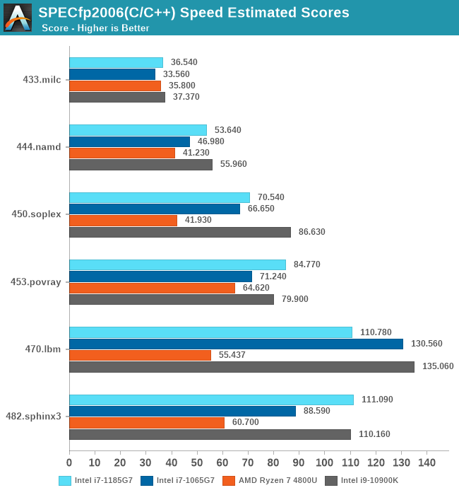
In the floating-point workloads, we again see the Tiger Lake chip doing extremely well, but there are some outliers. As mentioned 470.lbm is which is also extremely bandwidth hungry sees a generational degradation, which again could be L3 related, or something more specific to the memory subsystem.
There’s actually a wider IPC degradation in this set, with 482.sphinx being the only positive workload with a +2% boost, while the rest fall in a -12%, -7%, -14%, -3% and that massive -31% degradation for 470.lbm. Essentially, all workload which have stronger memory pressure characteristics.
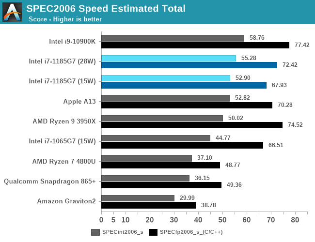
Overall SPEC2006 score performance for Tiger Lake is extremely good. Here we also present the 15W vs 28W configuration figures for the single-threaded workloads, which do see a jump in performance by going to the higher TDP configuration, meaning the design is thermally constrained at 15W even in ST workloads. By the way, this is a core power consumption limitation, as even small memory footprint workloads see a performance jump.
The i7-1185G7 is at the heels of the desktop i9-10900K, trailing only by a few percentage points.
Against the x86 competition, Tiger Lake leaves AMD’s Zen2-based Renoir in the dust when it comes to single-threaded performance. Comparing it against Apple’s A13, things aren’t looking so rosy as the Intel CPU barely outmatches it even though it uses several times more power, which doesn’t bode well for Intel once Apple releases its “Apple Silicon” Macbooks.
Even against Arm’s Cortex-A77 things aren’t looking rosy, as the x86 crowd just all that much ahead considering the Arm design only uses 2W.
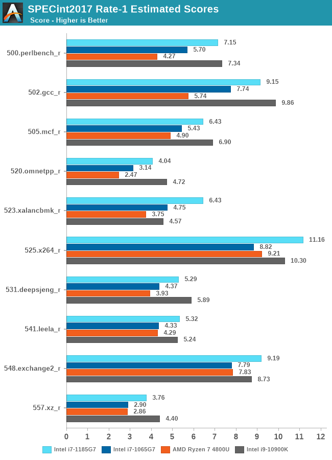
Moving onto the newer SPEC2017 suite, we’re seeing a quite similar story across the scaling between the platforms. Tiger Lake and its Willow Cove cores are showcasing outstanding performance as long as things are execution-bound, however do fall behind a bit to the desktop system when memory comes into play. There are two sets of results here, workloads which have high bandwidth or latency requirements, or those which have large memory footprint requirements.
523.xalancbmk_r seems to be of the latter as it’s posting a quite nice 10% IPC jump for Willow Cove while the rest generally in-between -4% regressions or +3-5% improvements.
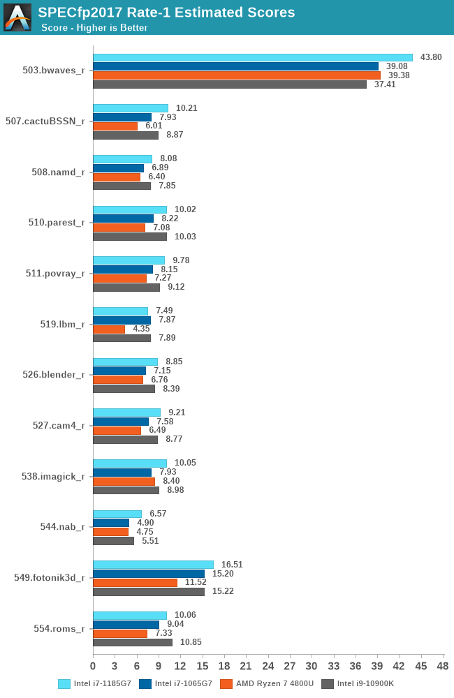
In the FP suite, we mostly see again the same kind of characteristics, with performance most of the time scaling in line with the clock frequency of Tiger Lake, with a few outliers here and there in terms of IPC, such as 544.nab_r gaining +9%, or 549.fotonik3d_r regressing by 12%.
Much like in the 2006 suite, the memory bandwidth hungry 519.lbm_r sees a 23% IPC regression, also regressing its absolute performance below that of Ice Lake.
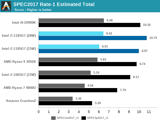
Overall, in the 2017 scores, Tiger Lake actually comes in as the leading CPU microarchitecture if you account both the integer and float-point scores together.
Although the design’s absolute performance here is exemplary, I feel a bit disappointed that in general the majority of the performance gains seen today were due to the higher clock frequencies of the new design.
IPC improvements of Willow Cove are quite mixed. In some rare workloads which can fully take advantage of the cache increases we’re seeing 9-10% improvements, but these are more of an exception rather than the rule. In other workloads we saw some quite odd performance regressions, especially in tests with high memory pressure where the design saw ~5-12% regressions. As a geometric mean across all the SPEC workloads and normalised for frequency, Tiger Lake showed 97% of the performance per clock of Ice Lake.
In a competitive landscape where AMD is set to make regular +15% generational IPC improvements and Arm now has an aggressive roadmap with yearly +30% IPC upgrades, Intel’s Willow Cove, although it does deliver great performance, seems to be a rather uninspiring microarchitecture.
Section by Andrei Frumusanu
CPU MT Performance: SPEC 2006, SPEC 2017
We’ve noted the earlier discussions of Intel’s TDP handling and how Tiger Lake has 15W and 28W operating modes, and where this comes into play the most is in multi-threaded scenarios where the platform is generally power envelope limited, having to otherwise clock down.
We’re showcasing the MT performance in SPEC for both the Tiger Lake modes, comparing it to both the 15W Ice Lake and AMD Renoir chips. As a note, the 15W Ice Lake platform had a sustained power draw of 18W which makes things not quite as apples-to-apples. Also as a reminder, the Intel systems have 4 cores and are running 8 thread instances, while the AMD system has 8 cores and is running 16 threads.
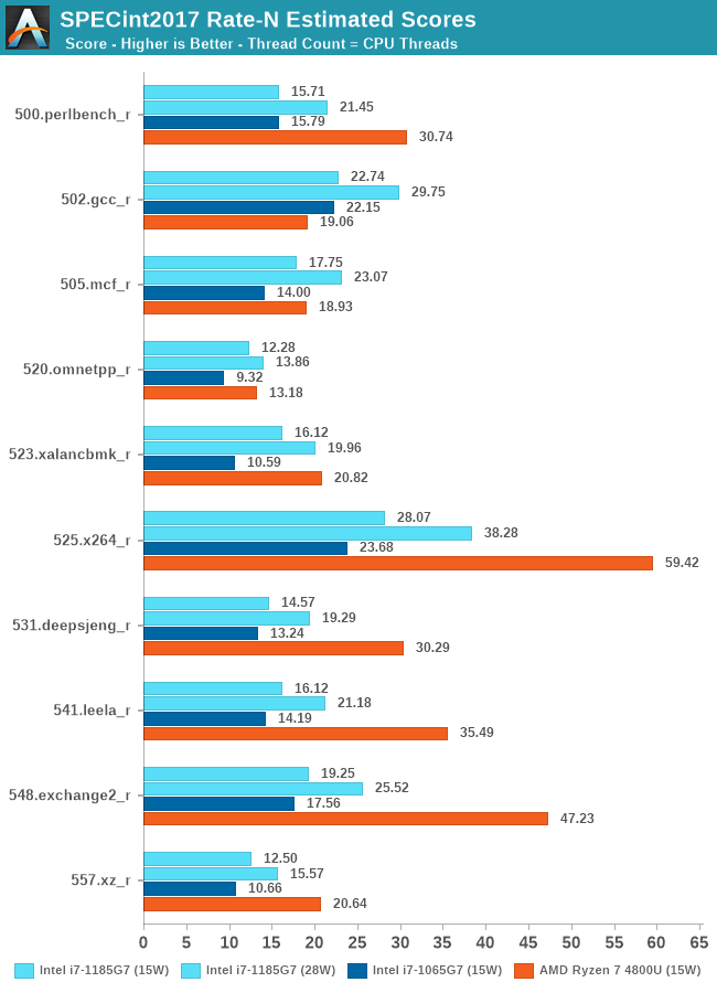
At first glance, the Tiger Lake system performs quite well versus its predecessor, but that’s mostly only in the 28W mode. At 15W, the generational boost, while it is there, isn’t that significant. This might point out that efficiency isn’t all that much better this generation.
AMD’s platform scales incredibly well in execution-bound workloads as it fully takes advantage of double the core count. In more memory-heavy workloads, the Zen2 cores here seem to be lacking sufficient resources and scale below the performance of Intel’s 4-core designs in some workloads.
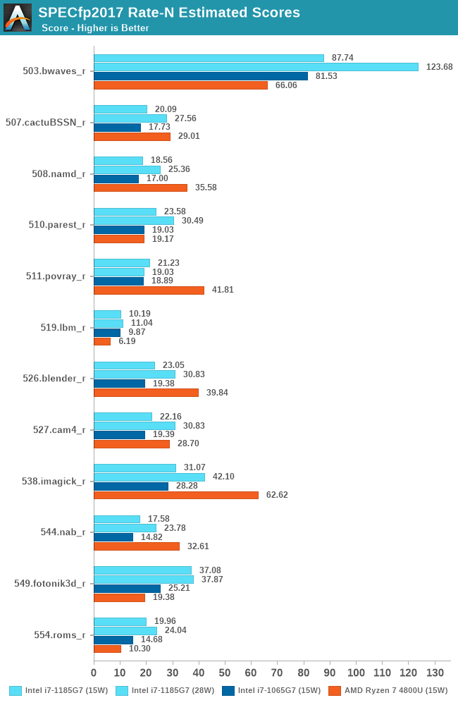
In the floating-point results, it’s again a matter of TDP headroom as well as memory performance scalability. In the 15W results, the Tiger Lake chip posts rather small improvements over its Ice Lake counterpart, whilst in the 28W mode the gains are more considerable and even manages to outperform the AMD system more often than not.
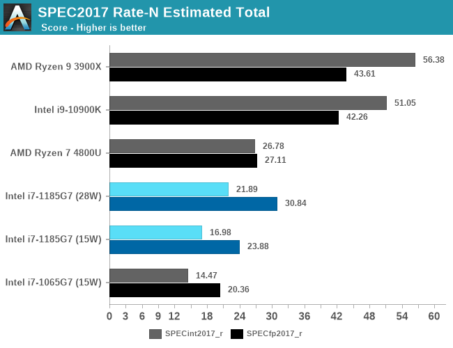
In the overall scores, the verdict on Tiger Lake is dependent on how you evaluate Intel’s performance gains. At an (semi)equal-TDP level between Tiger Lake and Ice Lake, the improvements in performance are 17%. Intel does reach a larger 51% generational performance boost in its 28W configuration, but at that point we’re talking about quite different cooling solutions inside of a laptop, no longer making this a valid apples-to-apples comparison.
We haven’t had opportunity to test out higher TDP -HS model of Renoir yet, but with the 15W 4800U already mostly tied with the 28W i7-1185G7, we would expect it to notably outperform the Tiger Lake chip.
Overall, Tiger Lake seems to be offering roughly 20% better performance per watt over its predecessor, with increased performance beyond that coming at a cost of higher power consumption.
CPU Performance: Office and Web
Our previous set of ‘office’ benchmarks have often been a mix of science and synthetics, so this time we wanted to keep our office section purely on real world performance.
Agisoft Photoscan 1.3.3: link
Photoscan stays in our benchmark suite from the previous benchmark scripts, but is updated to the 1.3.3 Pro version. As this benchmark has evolved, features such as Speed Shift or XFR on the latest processors come into play as it has many segments in a variable threaded workload.
The concept of Photoscan is about translating many 2D images into a 3D model - so the more detailed the images, and the more you have, the better the final 3D model in both spatial accuracy and texturing accuracy. The algorithm has four stages, with some parts of the stages being single-threaded and others multi-threaded, along with some cache/memory dependency in there as well. For some of the more variable threaded workload, features such as Speed Shift and XFR will be able to take advantage of CPU stalls or downtime, giving sizeable speedups on newer microarchitectures.
For the update to version 1.3.3, the Agisoft software now supports command line operation. Agisoft provided us with a set of new images for this version of the test, and a python script to run it. We’ve modified the script slightly by changing some quality settings for the sake of the benchmark suite length, as well as adjusting how the final timing data is recorded. The python script dumps the results file in the format of our choosing. For our test we obtain the time for each stage of the benchmark, as well as the overall time.
The final result is a table that looks like this:
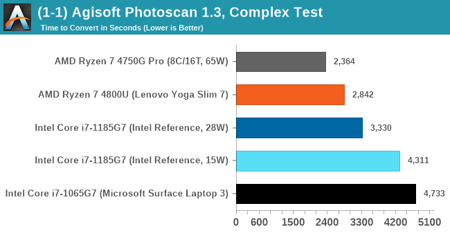
As explained in the power tests, the 4800U with double the cores wins out here, and due to the vector pressure also wins on power efficiency. There’s still a sizeable uplift from Ice Lake to Tiger Lake at 15 W, although 28 W is needed to get something sizeable.
Mozilla Kraken 1.1
Kraken is a 2010 benchmark from Mozilla and does a series of JavaScript tests. These tests are a little more involved than previous tests, looking at artificial intelligence, audio manipulation, image manipulation, json parsing, and cryptographic functions. The benchmark starts with an initial download of data for the audio and imaging, and then runs through 10 times giving a timed result.
Automation involves loading the direct webpage where the test is run and putting it through. All CPUs finish the test in under a couple of minutes, so we put that as the end point and copy the page contents into the clipboard before parsing the result. Each run of the test on most CPUs takes from half-a-second to a few seconds.
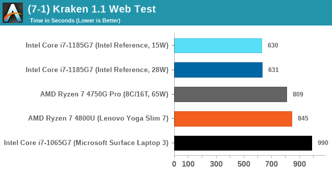
Both the Tiger Lake results are very fast, not showing much difference between the power modes. Intel pushes ahead of AMD here, and ultimately a sizable jump over Ice Lake.
Google Octane 2.0
Our second test is also JavaScript based, but uses a lot more variation of newer JS techniques, such as object-oriented programming, kernel simulation, object creation/destruction, garbage collection, array manipulations, compiler latency and code execution.
Octane was developed after the discontinuation of other tests, with the goal of being more web-like than previous tests. It has been a popular benchmark, making it an obvious target for optimizations in the JavaScript engines. Ultimately it was retired in early 2017 due to this, although it is still widely used as a tool to determine general CPU performance in a number of web tasks.
Octane’s automation is a little different than the others: there is no direct website to go to in order to run the benchmark. The benchmark page is opened, but the user has to navigate to the ‘start’ button or open the console and initiate the JavaScript required to run the test. The test also does not show an obvious end-point, but luckily does try and aim for a fixed time for each processor. This is similar to some of our other tests, that loop around a fixed time before ending. Unfortunately this doesn’t work if the first loop goes beyond that fixed time, as the loop still has to finish. For Octane, we have set it to 75 seconds per run, and we loop the whole test four times.
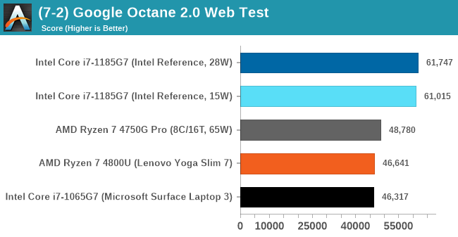
The Tiger Lake system reaches new records in Optane. If there’s anything this system is fast at, it is web workloads.
Speedometer 2: JavaScript Frameworks
Our newest web test is Speedometer 2, which is a test over a series of JavaScript frameworks to do three simple things: built a list, enable each item in the list, and remove the list. All the frameworks implement the same visual cues, but obviously apply them from different coding angles.
Our test goes through the list of frameworks, and produces a final score indicative of ‘rpm’, one of the benchmarks internal metrics. Rather than use the main interface, we go to the admin interface through the about page and manage the results there. It involves saving the webpage when the test is complete and parsing the final result.
We repeat over the benchmark for a dozen loops, taking the average of the last five.
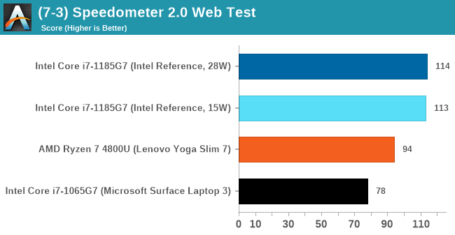
Again, another good win for Tiger Lake.
CPU Performance: Simulation and Science
Simulation and Science have a lot of overlap in the benchmarking world, however for this distinction we’re separating into two segments mostly based on the utility of the resulting data. The benchmarks that fall under Science have a distinct use for the data they output – in our Simulation section, these act more like synthetics but at some level are still trying to simulate a given environment.
DigiCortex v1.35: link
DigiCortex is a pet project for the visualization of neuron and synapse activity in the brain. The software comes with a variety of benchmark modes, and we take the small benchmark which runs a 32k neuron/1.8B synapse simulation, similar to a small slug.
The results on the output are given as a fraction of whether the system can simulate in real-time, so anything above a value of one is suitable for real-time work. The benchmark offers a 'no firing synapse' mode, which in essence detects DRAM and bus speed, however we take the firing mode which adds CPU work with every firing.
I reached out to the author of the software, who has added in several features to make the software conducive to benchmarking. The software comes with a series of batch files for testing, and we run the ‘small 64-bit nogui’ version with a modified command line to allow for ‘benchmark warmup’ and then perform the actual testing.
The software originally shipped with a benchmark that recorded the first few cycles and output a result. So while fast multi-threaded processors this made the benchmark last less than a few seconds, slow dual-core processors could be running for almost an hour. There is also the issue of DigiCortex starting with a base neuron/synapse map in ‘off mode’, giving a high result in the first few cycles as none of the nodes are currently active. We found that the performance settles down into a steady state after a while (when the model is actively in use), so we asked the author to allow for a ‘warm-up’ phase and for the benchmark to be the average over a second sample time.
For our test, we give the benchmark 20000 cycles to warm up and then take the data over the next 10000 cycles seconds for the test – on a modern processor this takes 30 seconds and 150 seconds respectively. This is then repeated a minimum of 10 times, with the first three results rejected.
We also have an additional flag on the software to make the benchmark exit when complete (which is not default behavior). The final results are output into a predefined file, which can be parsed for the result. The number of interest for us is the ability to simulate this system in real-time, and results are given as a factor of this: hardware that can simulate double real-time is given the value of 2.0, for example.
The final result is a table that looks like this:
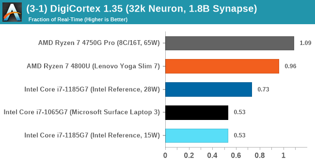
DigiCortex likes the 8-core AMD processors, but doesn't seem to like the LPDDR4 memory over the standard DDR4.
Dwarf Fortress 0.44.12: Link
Another long standing request for our benchmark suite has been Dwarf Fortress, a popular management/roguelike indie video game, first launched in 2006 and still being regularly updated today, aiming for a Steam launch sometime in the future.
Emulating the ASCII interfaces of old, this title is a rather complex beast, which can generate environments subject to millennia of rule, famous faces, peasants, and key historical figures and events. The further you get into the game, depending on the size of the world, the slower it becomes as it has to simulate more famous people, more world events, and the natural way that humanoid creatures take over an environment. Like some kind of virus.
For our test we’re using DFMark. DFMark is a benchmark built by vorsgren on the Bay12Forums that gives two different modes built on DFHack: world generation and embark. These tests can be configured, but range anywhere from 3 minutes to several hours. We’ve tested a large world generation scenario:
- Large, a 257x257 world with 550 years, 40 civilizations and 10 megabeasts
DFMark outputs the time to run any given test, so this is what we use for the output. We loop the large test for as many times in an hour.
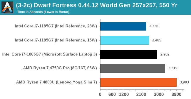
Intel's hardware likes Dwarf Fortress. It is primarily single threaded, and so a high IPC and a high frequency is what matters here.
Dolphin v5.0 Emulation: Link
Many emulators are often bound by single thread CPU performance, and general reports tended to suggest that Haswell provided a significant boost to emulator performance. This benchmark runs a Wii program that ray traces a complex 3D scene inside the Dolphin Wii emulator. Performance on this benchmark is a good proxy of the speed of Dolphin CPU emulation, which is an intensive single core task using most aspects of a CPU. Results are given in seconds, where the Wii itself scores 1051 seconds.
The Dolphin software has the ability to output a log, and we obtained a version of the benchmark from a Dolphin developer that outputs the display into that log file. The benchmark when finished will automatically try to close the Dolphin software (which is not normal behavior) and brings a pop-up on display to confirm, which our benchmark script can detects and remove. The log file is fairly verbose, so the benchmark script iterates through line-by-line looking for a regex match in line with the final time to complete.
The final result is a table that looks like this:
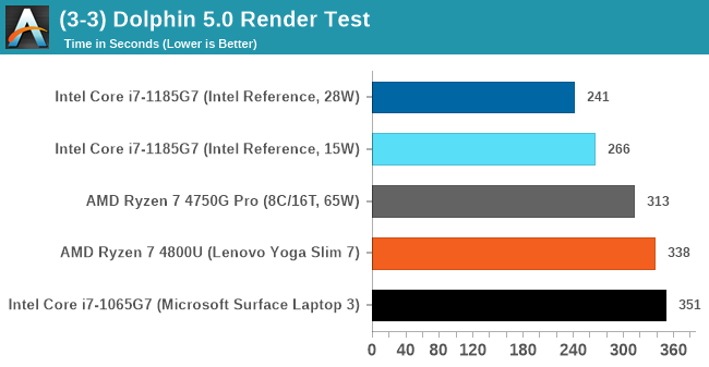
More often than not Intel's processors are the ones to choose for this sort of emulation - AMD catched up with Zen 2, but it would appear that Tiger Lake makes another leap forward.
CPU Tests: Science
In this version of our test suite, all the science focused tests that aren’t ‘simulation’ work are now in our science section. This includes Brownian Motion, calculating digits of Pi, molecular dynamics, and for the first time, we’re trialing an artificial intelligence benchmark, both inference and training, that works under Windows using python and TensorFlow. Where possible these benchmarks have been optimized with the latest in vector instructions, except for the AI test – we were told that while it uses Intel’s Math Kernel Libraries, they’re optimized more for Linux than for Windows, and so it gives an interesting result when unoptimized software is used.
3D Particle Movement v2.1: Non-AVX and AVX2/AVX512
This is the latest version of the benchmark designed to simulate semi-optimized scientific algorithms taken directly from my doctorate thesis. This involves randomly moving particles in a 3D space using a set of algorithms that define random movement. Version 2.1 improves over 2.0 by passing the main particle structs by reference rather than by value, and decreasing the amount of double->float->double recasts the compiler was adding in.
The initial version of v2.1 is a custom C++ binary of my own code, flags are in place to allow for multiple loops of the code with a custom benchmark length. By default this version runs six times and outputs the average score to the console, which we capture with a redirection operator that writes to file.
For v2.1, we also have a fully optimized AVX2/AVX512 version, which uses intrinsics to get the best performance out of the software. This was done by a former Intel AVX-512 engineer who now works elsewhere. According to Jim Keller, there are only a couple dozen or so people who understand how to extract the best performance out of a CPU, and this guy is one of them. To keep things honest, AMD also has a copy of the code, but has not proposed any changes.
The final result is a table that looks like this:
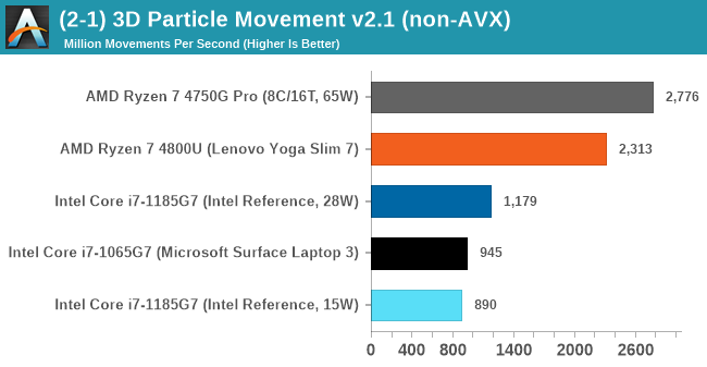
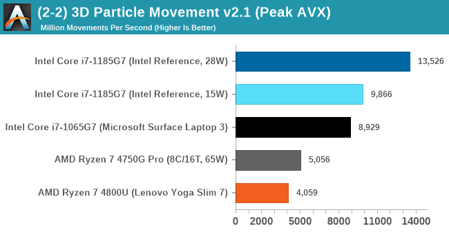
For the non-AVX compute, the eight cores of the AMD processors are ahead, however AVX-512 is a powerful tool in the right hands, with the 1185G7 offering 2x-3x performance for the same power than AMD.
y-Cruncher 0.78.9506: www.numberworld.org/y-cruncher
If you ask anyone what sort of computer holds the world record for calculating the most digits of pi, I can guarantee that a good portion of those answers might point to some colossus super computer built into a mountain by a super-villain. Fortunately nothing could be further from the truth – the computer with the record is a quad socket Ivy Bridge server with 300 TB of storage. The software that was run to get that was y-cruncher.
Built by Alex Yee over the last part of a decade and some more, y-Cruncher is the software of choice for calculating billions and trillions of digits of the most popular mathematical constants. The software has held the world record for Pi since August 2010, and has broken the record a total of 7 times since. It also holds records for e, the Golden Ratio, and others. According to Alex, the program runs around 500,000 lines of code, and he has multiple binaries each optimized for different families of processors, such as Zen, Ice Lake, Sky Lake, all the way back to Nehalem, using the latest SSE/AVX2/AVX512 instructions where they fit in, and then further optimized for how each core is built.
For our purposes, we’re calculating Pi, as it is more compute bound than memory bound.
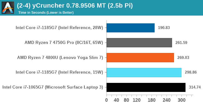
y-Cruncher takes advantage of the extra power available in the 28 W TDP mode, utilizing AVX-512 better than AMD can do with eight cores on AVX2 at 65 W.
NAMD 2.13 (ApoA1): Molecular Dynamics
One of the popular science fields is modelling the dynamics of proteins. By looking at how the energy of active sites within a large protein structure over time, scientists behind the research can calculate required activation energies for potential interactions. This becomes very important in drug discovery. Molecular dynamics also plays a large role in protein folding, and in understanding what happens when proteins misfold, and what can be done to prevent it. Two of the most popular molecular dynamics packages in use today are NAMD and GROMACS.
NAMD, or Nanoscale Molecular Dynamics, has already been used in extensive Coronavirus research on the Frontier supercomputer. Typical simulations using the package are measured in how many nanoseconds per day can be calculated with the given hardware, and the ApoA1 protein (92,224 atoms) has been the standard model for molecular dynamics simulation.
Luckily the compute can home in on a typical ‘nanoseconds-per-day’ rate after only 60 seconds of simulation, however we stretch that out to 10 minutes to take a more sustained value, as by that time most turbo limits should be surpassed. The simulation itself works with 2 femtosecond timesteps.
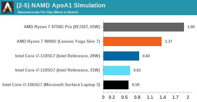
NAMD scales well with cores.
AI Benchmark 0.1.2 using TensorFlow: Link
Finding an appropriate artificial intelligence benchmark for Windows has been a holy grail of mine for quite a while. The problem is that AI is such a fast moving, fast paced word that whatever I compute this quarter will no longer be relevant in the next, and one of the key metrics in this benchmarking suite is being able to keep data over a long period of time. We’ve had AI benchmarks on smartphones for a while, given that smartphones are a better target for AI workloads, but it also makes some sense that everything on PC is geared towards Linux as well.
Thankfully however, the good folks over at ETH Zurich in Switzerland have converted their smartphone AI benchmark into something that’s useable in Windows. It uses TensorFlow, and for our benchmark purposes we’ve locked our testing down to TensorFlow 2.10, AI Benchmark 0.1.2, while using Python 3.7.6 – this was the only combination of versions we could get to work, because Python 3.8 has some quirks.
The benchmark runs through 19 different networks including MobileNet-V2, ResNet-V2, VGG-19 Super-Res, NVIDIA-SPADE, PSPNet, DeepLab, Pixel-RNN, and GNMT-Translation. All the tests probe both the inference and the training at various input sizes and batch sizes, except the translation that only does inference. It measures the time taken to do a given amount of work, and spits out a value at the end.
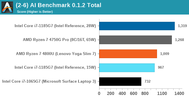
Intel currently has the easier tools for AI acceleration, and the developers here use the Intel Math Kernel Libraries. These libraries aren't to fond of scaling in windows compared to Linux, but we still see a sizeable uplift for Tiger Lake from Ice Lake.
CPU Performance: Encoding
One of the interesting elements on modern processors is encoding performance. This covers two main areas: encryption/decryption for secure data transfer, and video transcoding from one video format to another.
In the encrypt/decrypt scenario, how data is transferred and by what mechanism is pertinent to on-the-fly encryption of sensitive data - a process by which more modern devices are leaning to for software security.
Video transcoding as a tool to adjust the quality, file size and resolution of a video file has boomed in recent years, such as providing the optimum video for devices before consumption, or for game streamers who are wanting to upload the output from their video camera in real-time. As we move into live 3D video, this task will only get more strenuous, and it turns out that the performance of certain algorithms is a function of the input/output of the content.
HandBrake 1.32: Link
Video transcoding (both encode and decode) is a hot topic in performance metrics as more and more content is being created. First consideration is the standard in which the video is encoded, which can be lossless or lossy, trade performance for file-size, trade quality for file-size, or all of the above can increase encoding rates to help accelerate decoding rates. Alongside Google's favorite codecs, VP9 and AV1, there are others that are prominent: H264, the older codec, is practically everywhere and is designed to be optimized for 1080p video, and HEVC (or H.265) that is aimed to provide the same quality as H264 but at a lower file-size (or better quality for the same size). HEVC is important as 4K is streamed over the air, meaning less bits need to be transferred for the same quality content. There are other codecs coming to market designed for specific use cases all the time.
Handbrake is a favored tool for transcoding, with the later versions using copious amounts of newer APIs to take advantage of co-processors, like GPUs. It is available on Windows via an interface or can be accessed through the command-line, with the latter making our testing easier, with a redirection operator for the console output.
Finding the right combination of tests to use in our Handbrake benchmark is often difficult. There is no one test that covers all scenarios – streamers have different demands to production houses, then there’s video call transcoding that also requires some measure of CPU performance.
This time around, we’re probing a range of quality settings that seem to fit a number of scenarios. We take the compiled version of this 16-minute YouTube video about Russian CPUs at 1080p30 h264 and convert into two different files:
- 1080p30 to 480p30 ‘Discord’: x264, Max Rate 2100 kbps, High Profile 4.0, Medium Preset, 30 Peak FPS
- 1080p30 to 720p30 ‘YouTube’: x264, Max Rate 25000 kbps, High Profile 3.2, Medium Preset, 30 Peak FPS
We expect to see most mobile CPUs can manage (1) in realtime, but (2) might be a challenge.
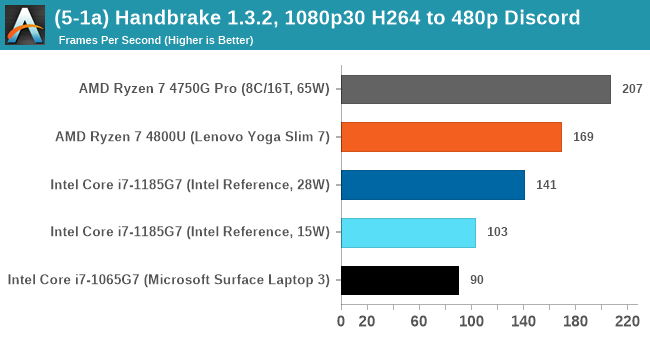

The extra cores of the AMD processor show through, with a small 12% jump from Ice to Tiger at 15W and a bigger jump moving to the 28 W mode.
WinRAR 5.90: Link
For the 2020 test suite, we move to the latest version of WinRAR in our compression test. WinRAR in some quarters is more user friendly that 7-Zip, hence its inclusion. Rather than use a benchmark mode as we did with 7-Zip, here we take a set of files representative of a generic stack
- 33 video files , each 30 seconds, in 1.37 GB,
- 2834 smaller website files in 370 folders in 150 MB,
- 100 Beat Saber music tracks and input files, for 451 MB
This is a mixture of compressible and incompressible formats. The results shown are the time taken to encode the file. Due to DRAM caching, we run the test for 20 minutes times and take the average of the last five runs when the benchmark is in a steady state.
For automation, we use AHK’s internal timing tools from initiating the workload until the window closes signifying the end. This means the results are contained within AHK, with an average of the last 5 results being easy enough to calculate.
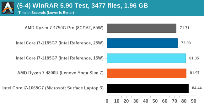
Along with single-core frequency, WinRAR benefits a lot from memory bandwidth as well as cache type. We have seen in past that the eDRAM enabled processors give a good benefit to software like WinRAR, and it is usually where we see the biggest DRAM differences. The Tiger Lake and 4800U use LPDDR4X-4266, with the Ice on LPDDR4X-3733. The extra power budget of the 28W mobile Tiger Lake seems to offer the most benefit.
CPU Tests: Rendering
Rendering tests, compared to others, are often a little more simple to digest and automate. All the tests put out some sort of score or time, usually in an obtainable way that makes it fairly easy to extract. These tests are some of the most strenuous in our list, due to the highly threaded nature of rendering and ray-tracing, and can draw a lot of power. If a system is not properly configured to deal with the thermal requirements of the processor, the rendering benchmarks is where it would show most easily as the frequency drops over a sustained period of time. Most benchmarks in this case are re-run several times, and the key to this is having an appropriate idle/wait time between benchmarks to allow for temperatures to normalize from the last test.
Blender 2.83 LTS: Link
One of the popular tools for rendering is Blender, with it being a public open source project that anyone in the animation industry can get involved in. This extends to conferences, use in films and VR, with a dedicated Blender Institute, and everything you might expect from a professional software package (except perhaps a professional grade support package). With it being open-source, studios can customize it in as many ways as they need to get the results they require. It ends up being a big optimization target for both Intel and AMD in this regard.
For benchmarking purposes, Blender offers a benchmark suite of tests: six tests varying in complexity and difficulty for any system of CPUs and GPUs to render up to several hours compute time, even on GPUs commonly associated with rendering tools. Unfortunately what was pushed to the community wasn’t friendly for automation purposes, with there being no command line, no way to isolate one of the tests, and no way to get the data out in a sufficient manner.
To that end, we fell back to one rendering a frame from a detailed project. Most reviews, as we have done in the past, focus on one of the classic Blender renders, known as BMW_27. It can take anywhere from a few minutes to almost an hour on a regular system. However now that Blender has moved onto a Long Term Support model (LTS) with the latest 2.83 release, we decided to go for something different.
We use this scene, called PartyTug at 6AM by Ian Hubert, which is the official image of Blender 2.83. It is 44.3 MB in size, and uses some of the more modern compute properties of Blender. As it is more complex than the BMW scene, but uses different aspects of the compute model, time to process is roughly similar to before. We loop the scene for 10 minutes, taking the average time of the completions taken. Blender offers a command-line tool for batch commands, and we redirect the output into a text file.
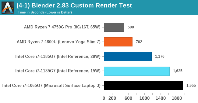
Blender takes advantage of the more cores, and the higher power limits.
Corona 1.3: Link
Corona is billed as a popular high-performance photorealistic rendering engine for 3ds Max, with development for Cinema 4D support as well. In order to promote the software, the developers produced a downloadable benchmark on the 1.3 version of the software, with a ray-traced scene involving a military vehicle and a lot of foliage. The software does multiple passes, calculating the scene, geometry, preconditioning and rendering, with performance measured in the time to finish the benchmark (the official metric used on their website) or in rays per second (the metric we use to offer a more linear scale).
The standard benchmark provided by Corona is interface driven: the scene is calculated and displayed in front of the user, with the ability to upload the result to their online database. We got in contact with the developers, who provided us with a non-interface version that allowed for command-line entry and retrieval of the results very easily. We loop around the benchmark five times, waiting 60 seconds between each, and taking an overall average. The time to run this benchmark can be around 10 minutes on a Core i9, up to over an hour on a quad-core 2014 AMD processor or dual-core Pentium.
One small caveat with this benchmark is that it needs online access to run, as the engine will only operate with a license from the licensing servers. For both the GUI and the command-line version, it does this automatically, but it does throw up an error if it can’t get a license. The good thing is that the license is valid for a week, so it doesn’t need further communications until that time runs out.
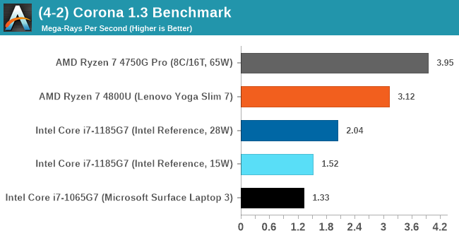
Corona is very similar to Blender in the performance scaling.
Crysis CPU-Only Gameplay
One of the most oft used memes in computer gaming is ‘Can It Run Crysis?’. The original 2007 game, built in the Crytek engine by Crytek, was heralded as a computationally complex title for the hardware at the time and several years after, suggesting that a user needed graphics hardware from the future in order to run it. Fast forward over a decade, and the game runs fairly easily on modern GPUs.
But can we also apply the same concept to pure CPU rendering? Can a CPU, on its own, render Crysis? Since 64 core processors entered the market, one can dream. So we built a benchmark to see whether the hardware can.
For this test, we’re running Crysis’ own GPU benchmark, but in CPU render mode. This is a 2000 frame test, with low settings. Initially we planned to run the test over several resolutions, however realistically speaking only 1920x1080 matters at this point.
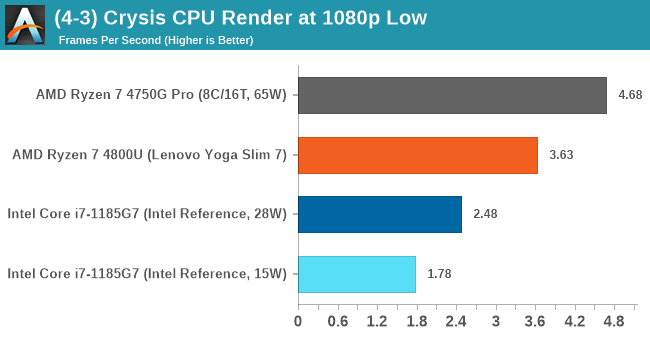
This benchmark is always amusing.
Xe-LP GPU Performance: Civilization VI
Originally penned by Sid Meier and his team, the Civilization series of turn-based strategy games are a cult classic, and many an excuse for an all-nighter trying to get Gandhi to declare war on you due to an integer underflow. Truth be told I never actually played the first version, but I have played every edition from the second to the sixth, including the fourth as voiced by the late Leonard Nimoy, and it a game that is easy to pick up, but hard to master.
Benchmarking Civilization has always been somewhat of an oxymoron – for a turn based strategy game, the frame rate is not necessarily the important thing here and even in the right mood, something as low as 5 frames per second can be enough. With Civilization 6 however, Firaxis went hardcore on visual fidelity, trying to pull you into the game. As a result, Civilization can taxing on graphics and CPUs as we crank up the details, especially in DirectX 12.
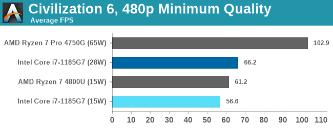
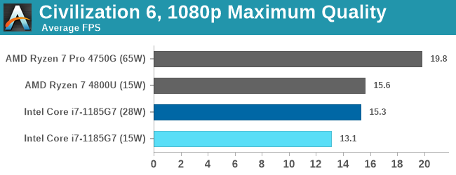
Civ6 is a game that enjoys lots of CPU performance, so we can see the desktop APU out front here. The eight cores of the 4800U get ahead of the 15 W version of Tiger Lake in both of our tests, although the 28 W power mode gets an 8% lead in the CPU-limited test.
Xe-LP GPU Performance: Deus Ex Mankind Divided
Deus Ex is a franchise with a wide level of popularity. Despite the Deus Ex: Mankind Divided (DEMD) version being released in 2016, it has often been heralded as a game that taxes the CPU. It uses the Dawn Engine to create a very complex first-person action game with science-fiction based weapons and interfaces. The game combines first-person, stealth, and role-playing elements, with the game set in Prague, dealing with themes of transhumanism, conspiracy theories, and a cyberpunk future. The game allows the player to select their own path (stealth, gun-toting maniac) and offers multiple solutions to its puzzles.
DEMD has an in-game benchmark, an on-rails look around an environment showcasing some of the game’s most stunning effects, such as lighting, texturing, and others. Even in 2020, it’s still an impressive graphical showcase when everything is jumped up to the max.
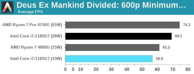
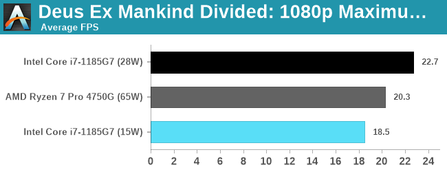
At the minimum settings, all of the integrated graphics are easily playable, with AMD winning at 15 W but the 28 W Tiger Lake goes a bit above that, within reaching distance of the desktop APU. At a more regular 1080p Maximum, the 20 FPS is perhaps a bit too slow for regular gameplay.
Xe-LP GPU Performance: Final Fantasy XIV
Despite being one number less than Final Fantasy 15, because FF14 is a massively-multiplayer online title, there are always yearly update packages which give the opportunity for graphical updates too. In 2019, FFXIV launched its Shadowbringers expansion, and an official standalone benchmark was released at the same time for users to understand what level of performance they could expect. Much like the FF15 benchmark we’ve been using for a while, this test is a long 7-minute scene of simulated gameplay within the title. There are a number of interesting graphical features, and it certainly looks more like a 2019 title than a 2010 release, which is when FF14 first came out.
With this being a standalone benchmark, we do not have to worry about updates, and the idea for these sort of tests for end-users is to keep the code base consistent.
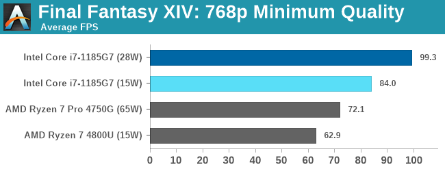
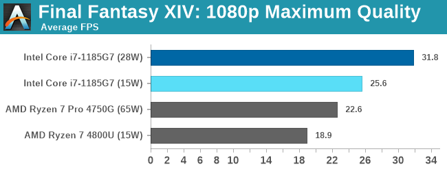
This is an easy win for Intel.
Xe-LP GPU Performance: Final Fantasy XV
Upon arriving to PC, Final Fantasy XV: Windows Edition was given a graphical overhaul as it was ported over from console. As a fantasy RPG with a long history, the fruits of Square-Enix’s successful partnership with NVIDIA are on display. The game uses the internal Luminous Engine, and as with other Final Fantasy games, pushes the imagination of what we can do with the hardware underneath us. To that end, FFXV was one of the first games to promote the use of ‘video game landscape photography’, due in part to the extensive detail even at long range but also with the integration of NVIDIA’s Ansel software, that allowed for super-resolution imagery and post-processing effects to be applied.
In preparation for the launch of the game, Square Enix opted to release a standalone benchmark. Using the Final Fantasy XV standalone benchmark gives us a lengthy standardized sequence to record, although it should be noted that its heavy use of NVIDIA technology means that the Maximum setting has problems - it renders items off screen. To get around this, we use the standard preset which does not have these issues. We use the standard quality settings.
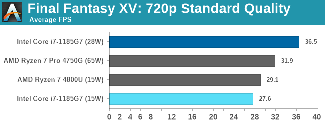

OK so testing at 8K was a complete accident. In that pure GPU limited scenario, Intel is ahead. When at 720p in a more standard combination of settings, Intel's 28 W goes above the 65 W desktop integrated graphics, but is behind when stuck in 15 W mode.
Xe-LP GPU Performance: World of Tanks
Albeit different to most of the other commonly played MMO or massively multiplayer online games, World of Tanks is set in the mid-20th century and allows players to take control of a range of military based armored vehicles. World of Tanks (WoT) is developed and published by Wargaming who are based in Belarus, with the game’s soundtrack being primarily composed by Belarusian composer Sergey Khmelevsky. The game offers multiple entry points including a free-to-play element as well as allowing players to pay a fee to open up more features. One of the most interesting things about this tank based MMO is that it achieved eSports status when it debuted at the World Cyber Games back in 2012.
World of Tanks enCore is a demo application for its new graphics engine penned by the Wargaming development team. Over time the new core engine has been implemented into the full game upgrading the games visuals with key elements such as improved water, flora, shadows, lighting as well as other objects such as buildings. The World of Tanks enCore demo app not only offers up insight into the impending game engine changes, but allows users to check system performance to see if the new engine runs optimally on their system. There is technically a Ray Tracing version of the enCore benchmark now available, however because it can’t be deployed standalone without the installer, we decided against using it. If that gets fixed, then we can look into it.
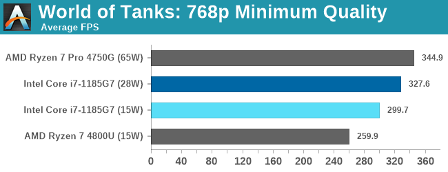
WoT is an easy win for Intel.
Xe-LP GPU Performance: F1 2019
The F1 racing games from Codemasters have been popular benchmarks in the tech community, mostly for ease-of-use and that they seem to take advantage of any area of a machine that might be better than another. The 2019 edition of the game features all 21 circuits on the calendar, and includes a range of retro models and DLC focusing on the careers of Alain Prost and Ayrton Senna. Built on the EGO Engine 3.0, the game has been criticized similarly to most annual sports games, by not offering enough season-to-season graphical fidelity updates to make investing in the latest title worth it, however the 2019 edition revamps up the Career mode, with features such as in-season driver swaps coming into the mix. The quality of the graphics this time around is also superb, even at 4K low or 1080p Ultra.
To be honest, F1 benchmarking has been up and down in any given year. Since at least 2014, the benchmark has revolved around a ‘test file’, which allows you to set what track you want, which driver to control, what weather you want, and which cars are in the field. In previous years I’ve always enjoyed putting the benchmark in the wet at Spa-Francorchamps, starting the fastest car at the back with a field of 19 Vitantonio Liuzzis on a 2-lap race and watching sparks fly. In some years, the test file hasn’t worked properly, with the track not being able to be changed.
For our test, we put Alex Albon in the Red Bull in position #20, for a dry two-lap race around Austin.
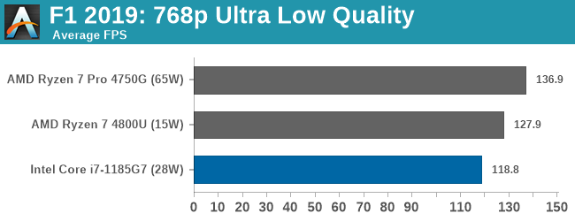
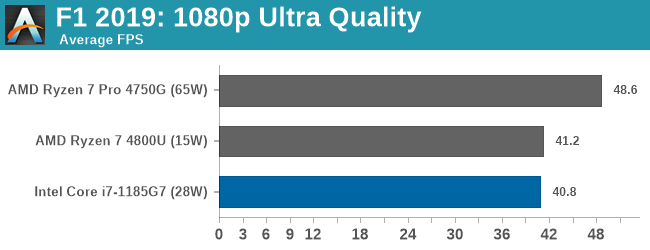
In this case, at 1080p Ultra, AMD and Intel (28W) are matched. Unfortunately looking through the data, the 15 W test run crashed and we only noticed after we returned the system.
Conclusion: Is Intel Smothering AMD in Sardine Oil?
Whenever a new processor family is reviewed, it is easy to get caught up in the metrics. More performance! Better power consumption! Increased efficiency! Better clock-for-clock gains! Amazing price! Any review through a singular lens can fall into the trap of only focusing on that specific metric. So which metrics matter more than others? That depends on who you are and what the product is for.
Tiger Lake is a mobile processor, featuring Intel's fastest cores and new integrated graphics built with an updated manufacturing process. This processor will be cast into the ultra-premium notebook market, as it carries the weight of the best Intel has to offer across a number of its engineering groups. Intel is actively working with its partners to build products to offer the best in performance for this segment right before a discrete GPU is absolutely needed.
As a road warrior, pairing the right performance with power efficiency is a must. In our benchmarks, due to the new process node technology as well as the updated voltage/frequency scaling, we can see that Tiger Lake offers both better performance at the same power compared to Ice Lake, but it also extends the range of performance over Ice Lake, assisted by that much higher turbo boost frequency of 4.8 GHz. When Tiger Lake gets into retail systems, particularly at the 15 W level, it is going to be fun to see what sort of battery life improvements during real-world workflows are observed.
As an engineer, genuine clock-for-clock performance gains get me excited. Unfortunately Tiger Lake doesn't deliver much on this front, and in some cases, we see regressions due to the rearranged cache depending on the workload used. This metric ignores power - but power is the metric on which Tiger Lake wins. Intel hasn't really been wanting to talk about the raw clock-for-clock performance, and perhaps understandably so (from a pure end-user product point of view at any rate).
Tiger Lake has updates for security as well as Control-Flow Enforcement Technology, which is a good thing, however these are held behind the vPro versions, creating additional segmentation in the product stack on the basis of security features. I’m not sure I approve of this, potentially leaving the non-vPro unsecure and trying to upsell business customers for the benefit.
The new Tiger Lake stills falls down against the competition when we start discussing raw throughput tests. Intel was keen to promote professional workflows with Tiger Lake, or gaming workflows such as streaming, particularly at 28 W rather than at 15 W. Despite this we can easily see that the 15 W Renoir options with eight cores can blow past Tiger Lake in a like-for-like scenario in our rendering tests and our scalable workloads. The only times Intel scores a win is due to accelerator support (AVX-512, DP4a, DL Boost). On top of that, Renoir laptops in the market are likely to be in a cheaper price bracket than what Intel seems to be targeting.
If Intel can convince software developers to jump on board with using its accelerators, then both the customers will benefit as will Intel’s metrics. The holy grail may be when it comes to OneAPI, enabling programmers to target different aspects of Intel’s eco-system under the same toolset. However OneAPI is only just entering v1.0, and any software project base building like that requires a few years to get off the ground.
For end-user performance, Tiger Lake is going to offer a good performance improvement over Ice Lake, or the same performance at less power. It’s hard to ignore. If Intel’s partners can fit 28 W versions of the silicon into the 15 W chassis they were using for Ice Lake, then it should provide for a good product.
We didn’t have too much time to go into the performance of the new Xe-LP graphics, although it was clear to see that the 28 W mode does get a good performance lift over the 15 W mode, perhaps indicating that DG1 (the discrete graphics coming later) is worth looking out for. Against AMD’s best 15 W mobile processor and integrated graphics, our results perhaps at the lower resolutions were skewed towards AMD, but the higher resolutions were mostly wins for Intel - it seemed to vary a lot depending on the game engine.
As a concept, Tiger Lake’s marketing frustrates me. Not offering apples-to-apples data points and claiming that TDP isn’t worth defining as a singular point is demonstrating the lengths that Intel believes it has to go to in order to redefine its market and obfuscate direct comparisons. There was a time and a place where Intel felt the need to share everything, as much as possible, with us. It let us sculpt the story of where we envisaged the market was going, and OEMs/customers were on hand to add their comments about the viewpoints of the customer base from their perspective. It let us as the press filter back with comments, critiques, and suggestions. The new twist from Intel’s client division, one that’s actually been progressing along this quagmire path, will only serve to confuse its passionate customer base, its enthusiasts, and perhaps even the financial analysts.
However, if we’re just talking about the product, I’m in two minds for Tiger Lake. It doesn’t give those raw clock-for-clock performance gains that I’d like, mostly because it’s almost the same design as Ice Lake for the CPU cores, but the expansion of the range of performance coupled with the energy efficiency improvements will make it a better product overall. I didn’t believe the efficiency numbers at first, but successive tests showed good gains from both the manufacturing side of Intel as well as the silicon design and the power flow management. Not only that, the new Xe-LP graphics seem exciting, and warrant a closer inspection.
Tiger Lake isn’t sardine oil basting AMD just yet, but it stands to compete well in a number of key markets.

