Original Link: https://www.anandtech.com/show/16823/intel-accelerated-offensive-process-roadmap-updates-to-10nm-7nm-4nm-3nm-20a-18a-packaging-foundry-emib-foveros
Intel's Process Roadmap to 2025: with 4nm, 3nm, 20A and 18A?!
by Dr. Ian Cutress on July 26, 2021 5:00 PM EST
In today’s Intel Accelerated event, the company is driving a stake into the ground regarding where it wants to be by 2025. CEO Pat Gelsinger earlier this year stated that Intel would be returning to product leadership in 2025, but hasn’t yet explained how this is coming about – that is until today, where Intel has disclosed its roadmap for its next five generations of process node technology leading to 2025. Intel believes it can follow an aggressive strategy to match and pass its foundry rivals, while at the same time developing new packaging offerings and starting a foundry business for external customers. On top of all this, Intel has renamed its process nodes.
The Short Answer:
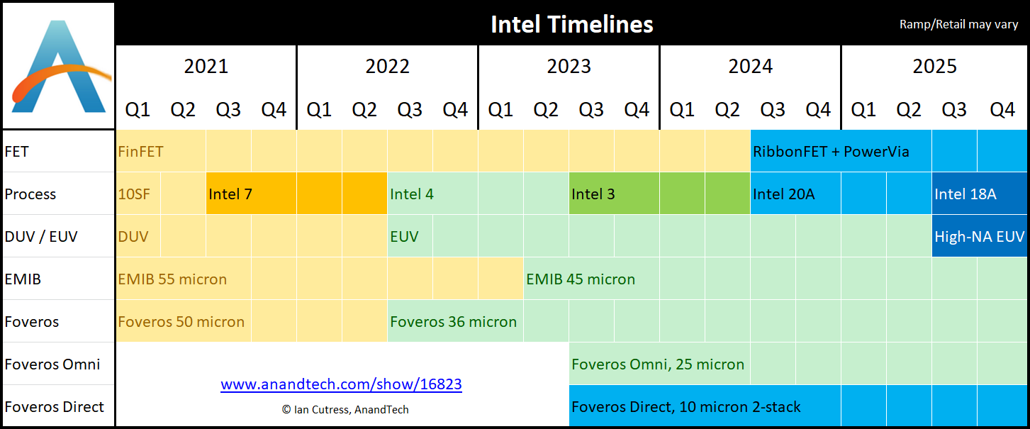
If you only take one thing away from this article, I'm going to put it here front and center. Here is what we're seeing for Intel's roadmaps, based on their disclosures today.
As always, there is a difference between when a technology ramps for production and comes to retail; Intel spoke about some technologies as 'being ready', while others were 'ramping', so this timeline is simply those dates as mentioned. As you might imagine, each process node is likely to exist for several years, this graph is simply showcasing the leading technology from Intel at any given time.
If you want the details on this graph, then read on.
Intel's Defines a Strong Future: Is TSMC at Risk?
Earlier this year, CEO Pat Gelsinger announced Intel’s new IDM 2.0 strategy, consisting of three elements:
- Build (7nm)
- Expand (TSMC)
- Productize (Intel Foundry Services)
The goal here is to continue to work on Intel’s process node technology development, going beyond the current 10nm designs in production today, but simultaneously using other foundry services from partners (or competitors) to regain/retain Intel’s position in its processors that drive a lot of the company revenue. The third element is IFS, Intel’s Foundry Services, where Intel is committing in a big way to opening up its manufacturing facilities to external semiconductor business.
Underpinning (1) and (3) is how Intel executes on its own process node development. While in Intel’s recent Q3 2021 earnings call CEO Gelsinger confirmed that Intel is now producing more 10nm wafers in a day than 14nm wafers, marking a shift in confidence between the two designs, it is no secret that Intel has had difficulty in transitioning from its 14nm process to its 10nm process. On June 29th this year, Intel also stated that its next generation 10nm product requires additional validation time to streamline deployment on enterprise systems for 2022. Note that at the same time, TSMC has surpassed Intel by shipping at capacity with its equivalent designs (called 7nm) and its leading edge (5nm) designs that surpass Intel’s performance.
As with the previous announcement in March, Intel is reaffirming that it intends to return to leadership performance in semiconductors in 2025. This will enable both the company to compete better as it builds its own products (1) but also offer a wider portfolio of performance and technologies for its future IFS customers (3). To do this, it is realigning the roadmap for its future process node technologies to be more aggressive with improvements, yet at the same time more modular with its technology to enable faster transitions.
Leading up this plan is Dr. Ann B Kelleher, who was named SVP and GM of the Technology Development division at Intel last year. This division is where all the research and development of Intel’s future process node technologies and enhancements comes from – it used to be part of Intel’s System Architecture Group, however it was split in July 2020 to re-establish a focus purely on Technology Development. Dr. Kelleher’s background involves process research in academia, followed by 26 years at Intel as a process engineer, moving up to managing Fab 24 in Ireland, Fab 12 in Arizona, Fab 11X in Rio Rancho, before landing in HQ in Oregon as the GM of Manufacturing and Operations.
Her experience covering both fab-scale production and process node research is going to be critical for Intel’s future plans. In discussing with Kelleher ahead of today’s announcements, she stated that she has implemented fundamental changes when it comes to supplier approach, ecosystem learnings, organizational changes, modular design strategies, contingency plans, and realigning the Technology Development Team into a more streamlined outfit ready to execute. These include key personnel such as Sanjay Natarajan as SVP and GM of Logic Development (one of Intel’s recent rehires) and Babak Sabi as CVP and GM of Assembly/Test Development
Intel is today defining ‘technology leadership by 2025’ as defined by the metric of performance per watt. We asked Intel is a pre-briefing what that means for peak performance, which is often a metric we care about for end product design, and the answer was that "peak performance remains a key part of Intel’s strategic development".
Intel Renames The Nodes: ‘Mine is Smaller’
The problem with simply posting Intel’s roadmap here is that the news is two-fold. Not only is Intel disclosing the state of its technology for the next several years, but the names of the technology are changing to better align with common industry norms.
It is no secret that having "Intel 10nm" being equivalent to "TSMC 7nm", even though the numbers actually have nothing to do with the physical implementation, has ground at Intel for a while. A lot of the industry, for whatever reason, hasn’t learned that these numbers aren’t actually a physical measurement. They used to be, but when we moved from 2D planar transistors to 3D FinFET transistors, the numbers became nothing more than a marketing tool. Despite this, every time there’s an article about the technology, people get confused. We’ve been talking about it for half a decade, but the confusion still remains.
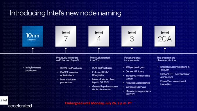
To that end, Intel is renaming its future process nodes. Here’s the roadmap image, but I’ll be breaking it down piece by piece.
2020, Intel 10nm SuperFin (10SF): Current generation technology in use with Tiger Lake and Intel’s Xe-LP discrete graphics solutions (SG1, DG1). The name stays the same.
2021 H2, Intel 7: Previously known as 10nm Enhanced Super Fin or 10ESF. Alder Lake and Sapphire Rapids will now be known as Intel 7nm products, showcasing a 10-15% performance per watt gain over 10SF due to transistor optimizations. Alder Lake is currently in volume production. Intel’s Xe-HP will now be known as an Intel 7 product.
2022 H2, Intel 4: Previously known as Intel 7nm. Intel earlier this year stated that its Meteor Lake processor will use a compute tile based on this process node technology, and the silicon is now back in the lab being tested. Intel expects a 20% performance per watt gain over the previous generation, and the technology uses more EUV, mostly in the BEOL. Intel’s next Xeon Scalable product, Granite Rapids, will also use a compute tile based on Intel 4.
2023 H2, Intel 3: Previously known as Intel 7+. Increased use of EUV and new high density libraries. This is where Intel’s strategy becomes more modular – Intel 3 will share some features of Intel 4, but enough will be new enough to describe this a new full node, in particular new high performance libraries. Nonetheless, a fast follow on is expected. Another step up in EUV use, Intel expects a manufacturing ramp in the second half of 2023 with an 18% performance per watt gain over Intel 4.
2024, Intel 20A: Previously known as Intel 5nm. Moving to double digit naming, with the A standing for Ångström, or 10A is equal to 1nm. Few details, but this is where Intel will move from FinFETs to its version of Gate-All-Around (GAA) transistors called RibbonFETs. Also Intel will debut a new PowerVia technology, described below.
2025, Intel 18A: Not listed on the diagram above, but Intel is expecting to have an 18A process in 2025. 18A will be using ASML’s latest EUV machines, known as High-NA machines, which are capable of more accurate photolithography. Intel has stated to us that it is ASML’s lead partner when it comes to High-NA, and is set to receive the first production model of a High-NA machine. ASML recently announced High-NA was being delayed- when asked if this was an issue, Intel said no, as the timelines for High-NA and 18A are where Intel expects to intersect and have unquestioned leadership.
Intel has confirmed to us that Intel 3 and Intel 20A will be offered to foundry customers (but hasn’t stated if Intel 4 or Intel 7 will be).
To bring this altogether in a single table, with known products, we have the following:
| Intel's Process Node Technology | ||||
| Old Name | New Name | Roadmap | Products | Features |
| 10SF | 10SF | Today | Tiger Lake SG1 DG1 Xe-HPC Base Tile Agilex-F/I FPGA |
SuperMIM Thin Film Barrier Volume 10nm On sale today |
| 10ESF | Intel 7 | 2021 H2 products | Alder Lake (21) Raptor Lake (22)? Sapphire Rapids (22) Xe-HP Xe-HPC IO Tile |
10-15% PPW Upgraded FinFET ADL in Ramp today |
| 7nm | Intel 4 | 2022 H2 ramp 2023 H1 products |
Meteor Compute Tile Granite Compute Tile |
20% PPW vs 7 More EUV Silicon in Lab |
| 7+ | Intel 3 | 2023 H2 products | - | 18% PPW vs 4 Area Savings More EUV New Perf Libraries Faster Follow On |
| 5nm | Intel 20A | 2024 | - | RibbonFET PowerVia |
| 5+ | Intel 18A | 2025 | Unquestioned Leadership | 2nd Gen Ribbon High NA EUV |
One of the issues here is the difference between a process node being ready, ramping production for product launches, and actually being made available. For example, Alder Lake (now on Intel 7nm) is due to come out this year, but Sapphire Rapids is going to be more of a 2022 product. Similarly, there are reports of Raptor Lake on Intel 7 coming out in 2022 to replace Alder Lake with the tiled Meteor Lake on Intel 4 in 2023. While Intel is happy to discuss process node development time frames, product timeframes are not as open (as no doubt customers would get frustrated if the time stated is missed).
Why The Nodes Were Renamed
So as stated before, one element of renaming the nodes is due to matching parity with other foundry offerings. Both TSMC and Samsung, competitors to Intel, were using smaller numbers to compare similar density processes. With Intel now renaming itself, it gets more in-line with the industry. That being said, perhaps sneakily, Intel’s 4nm might be on par with TSMC’s 5nm, reversing the tables. By 3nm we expect there to be a good parity point, however that will depend on Intel matching TSMC’s release schedule.
Rather than throw process node names everywhere, it is typical to refer to peak quoted transistor densities instead. Here is the table we published in our recent IBM 2nm news post, but with an updated shift on Intel’s naming.
| 2021 Peak Quoted Transistor Densities (MTr/mm2) | ||||
| AnandTech Process Name |
IBM | TSMC | Intel | Samsung |
| 22nm | 16.50 | |||
| 16nm/14nm | 28.88 | 44.67 | 33.32 | |
| 10nm | 52.51 | 100.76 | 51.82 | |
| 7nm | 91.20 | 100.76 | 95.08 | |
| 5/4nm | 171.30 | ~200* | 126.89 | |
| 3nm | 292.21* | |||
| 2nm / 20A | 333.33 | |||
| Data from Wikichip, Different Fabs may have different counting methodologies * Estimated Logic Density |
||||
Exactly where Intel’s new 4nm and below will end up is yet to be disclosed, as numbers with stars alongside are based on estimates by the respective companies.
It has been expected for a while that Intel would be realigning its process node naming. Behind closed doors, I personally have been lobbying for it for a while, and I know that a few other journalists and analysts have been suggesting it to Intel as well. Some responses we received were related to apathy – one executive told me that "our customers that care about this actually know the difference", which is true for sure, but what we’re talking about here is more about perception in the wider ecosystem for enthusiasts and financial analysts who might not be up to speed. It is more or less a branding exercise, and I also told Intel that they are going to have to expect a mixed response – some voices might interpret the move as Intel trying to pull one over on the market, for example. But they’re going to have to live with it, as these are the new names.
Meanwhile, despite Intel’s struggles with 10nm, it is still a process node in production and in volume production, in use for both consumer and enterprise devices, and it's coming to desktops very soon. Even though it has some stiff competition from other players, it is still an offering in the market, and for those that want to compare process node densities using these names, it should have a moniker to avoid confusion. I am applauding that Intel is doing it sooner rather than later.
One key point to note is that the new Intel 7 node, which was formerly the 10ESF node, is not necessarily a "full" node update as we typically understand it. This node is derived as an update from 10SF, and as the diagram above states, will have ‘transistor optimizations’. Moving from 10nm to 10SF, that meant SuperMIM and new thin-film designs giving an extra 1 GHz+, however the exact details from 10SF to the new Intel 7 is unclear at this point. Intel has however stated that moving from Intel 7 to Intel 4 will be a regular full node jump, with Intel 3 using modular parts of Intel 4 with new high-performance libraries and silicon improvements for another jump in performance.
We asked Intel if these process nodes will have additional optimization points, and were told that they will – whether any of them will be explicitly productized will depend on the features. Individual optimizations may account for an additional 5-10% performance per watt, and we were told that even 10SF (which keeps its name) has had several additional optimization points that haven’t necessarily been publicized. So whether these updates get marketed as 7+ or 7SF or 4HP is not known, but as with any manufacturing process as updates occur to help improve performance/power/yield, they get applied assuming the design adheres to the same rules.
"Isn't Intel Just Trying To Pull The Wool Over Our Eyes?"
No.
The problem here is that there is no consistent node naming between foundries. Intel has been saving any number change for major advances in its node manufacturing technology, instead using +/++ to signify improvements. If we compare this to TSMC and Samsung, both of whom have been happy to give half-node jumps new numbers entirely.
For example, Samsung's 7LPP is a major node, however 6LPP, 5LPE and 4LPE are all iterative efforts on the same design (arguably also iterative of 8LPP), with 3GAE being the next major jump. Compare this to Intel, who was planning 10nm to 7nm to 5nm as major process node jumps – so while Samsung had one jump planned and 4 sub-variants (or more), Intel had two major jumps. Similarly, TSMC's 10nm was a half-node jump over 16nm, while 16nm to 7nm was the full node – Intel made 14 to 10 to 7 as full nodes.
Intel stuck to its guns a long while, and delays to 10nm effectively hurt it in a multiplicative fashion. For example, if Intel had labeled 14+ as 13nm, and 14++ as 12nm, perhaps it wouldn't be so bad. I mean, yes Intel should expect some hurt for 10nm being late, but when other foundries were showcasing smaller steps as full number jumps, it became a marketing and media nightmare. 14++++ became an industry joke, and coupled with how every time when they talked about future process nodes they had to cite the equivalent TSMC of Samsung process, it got a bit too much. It had to be explained every time, as new people come into the industry.
I've lobbied Intel to adjust its naming for a while, and I know other peers have as well. When we refer to Intel 7 from now on, we can draw equivalents to TSMC 7nm (even if TSMC is shipping 5nm in volume) without having to extensively explain differences in a simple name. This isn't Intel pulling the wool over your eyes, or trying to hide a bad situation. This is Intel catching up to the rest of the industry in how these processes are named. To add to this, it's a good thing that Intel is only renaming future nodes that haven't reached the market yet.
This is a multi-page article!
Click the dropdown below for more pages, including
- This Page, New Node Names
- A Sidebar on Intel EUV and becoming ASML Lead Partner
- New for 2024: RibbonFETs and PowerVias
- Next Gen EMIB and Foveros Packaging
- Customers Customers Customers
Sidebar on Intel EUV
In all of these announcements, one thing to highlight is Intel mentioning its relationship with ASML, the sole company that manufactures the EUV machines powering production of leading edge semiconductor manufacturing.
ASML is a unique company in that it is the only one that can produce these machines, because the technology behind them is often tied up with its partners and research, but also because all the major silicon manufacturers are heavily invested in ASML. For any other company to compete against ASML would require building a separate network of expertise, a decade of innovation and design, and a lot of capital. None of the major silicon vendors want to disturb this balance and go off on their own, lest it shuts them out of the latest manufacturing technology, and no research fund sees competing against the embedded norm as a viable opportunity. This means that anyone wanting EUV specialist technology has to go to ASML.
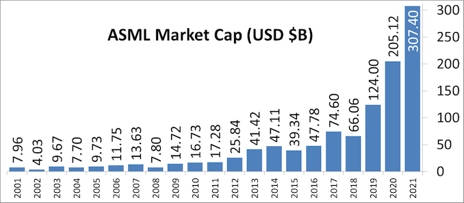
In 2012, it was reported that Intel, Samsung, and TSMC all invested in ASML. This was, at the time, to jumpstart EUV development along with migrating from 300mm wafers to 450mm wafers. While we haven’t moved to 450mm wafers yet (and there are doubts we will any time in the next decade), EUV is now here. Intel’s 2012 investment of $2.1 billion gave them a 10% stake in ASML, with Intel stating that it would continue investing up to a 25% stack. Those stakes are now below the 5% reporting threshold, but all three of the major foundry customers are still big owners, especially as ASML’s market cap has risen from $24 Billion in 2012 to $268 Billion in 2021 (surpassing Intel).
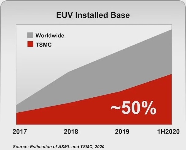
As major investors but also ASML’s customers, the race has been on for these foundries to acquire enough EUV machines to meet demand. TSMC reported in August 2020 that it has 50% of all EUV machines manufactured at ASML for its leading edge processes. Intel is a little behind, especially as none of Intel’s products in the market yet use any EUV. EUV will only intercept Intel’s portfolio with its new Intel 4 process, where it will be used extensively, mostly on the BEOL. But Intel still has to order machines when they need them, especially as there are reports that ASML currently has backorders of 50 EUV machines. In 2021, ASML is expected to manufacture around 45-50 machines, and 50-60 in 2022. The exact number of machines Intel has right now, or has ordered from ASML, is unknown. It is expected that each one has a ~$150m price tag, and can take 4-6 months to install.
With all that being said, Intel’s discussion point today is that it will be the lead customer for ASML’s next generation EUV technology known as High-NA EUV. NA in this context relates to the ‘numerical aperture’ of the EUV machine, or to put simply, how wide you can make the EUV beam inside the machine before it hits the wafer. The wider the beam before you hit the wafer, the more intense it can be when it hits the wafer, which increases how accurately the lines are printed. Normally in lithography to get better printed lines, we move from single patterning to double patterning (or quad patterning) to get that effect, which decreases yield. The move to High-NA would mean that the ecosystem can stay on single patterning for longer, which some have quoted as allowing the industry to ‘stay aligned with Moore’s Law longer’.
| ASML's EUV Shipments | |||||||||||||||||||||
| 2015 | 2016 | 2017 | 2018 | 2019 | 2020 | 2021 | |||||||||||||||
| Actual | 2 | 4 | 10 | 3 | 4 | 5 | 6 | 4 | 7 | 7 | 8 | 4 | 7 | 14 | 8 | 7 | 9 | - | - | ||
| Target (Total) | - | - | - | 20 (18) | 30 (26) | 35 (33) | 45-50 | ||||||||||||||
| 2018 and beyond is split per quarter for actual shipped numbers Data taken from ASML's Financial Reports |
|||||||||||||||||||||
Current EUV systems are NA 0.33, while the new systems are NA 0.55. ASML’s latest update suggests that it expects customers to be using High-NA for production in 2025/2026, which means that Intel is likely going to be getting the first machine (ASML NXE:5000 we think) in mid-2024. Exactly how many High-NA machines ASML intends to produce in that time frame is unknown, as if they flood the market, having the first won’t be a big win. However if there is a slow High-NA ramp, it will be up to Intel to capitalize on its advantage.
New Technology Features for 2024: RibbonFETs
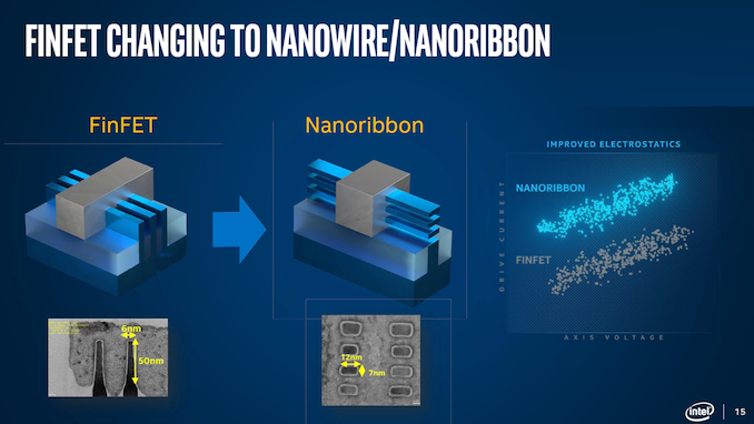
One of the major features of this roadmap is highlighted when it shifts to 20A, Intel’s process name referring to Angstroms rather than nanometers. At this juncture, as mentioned above, Intel will be transitioning from its FinFET design over to a new type of transistor, known as a Gate-All-Around transistor, or GAAFET. In Intel’s case, the marketing name they are giving their version is RibbonFET.
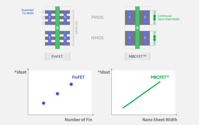
It has been widely expected that once the standard FinFET runs out of steam that the semiconductor manufacturing industry will pivot to GAAFET designs. Each of the leading edge vendors call their implementation something different (RibbonFET, MBCFET), but it is all using the same basic principle – a flexible width transistor with a number of layers helping drive transistor current. Where FinFETs relies on multiple quantized fins for source/drain and a cell height of multiple tracks of fins, GAAFETs enable a single fin of variable length, allowing the current for each individual cell device to be optimized in power, performance, or area.
Intel has been discussing GAAFETs in technical semiconductor conferences for a number of years, at the International VLSI conference in June 2020, then CTO Dr. Mike Mayberry showcased a diagram with the enhanced electrostatics of moving to a GAA design. At the time we asked about Intel’s timescale for implementing GAA in volume, and were told to expect them ‘within 5 years’. At present Intel’s RibbonFET is due to come with the 20A process, likely to be productized by the end of 2024 based on the roadmaps outlined above.
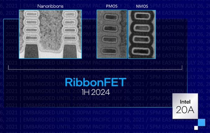
In Intel’s RibbonFET diagrams for this event, they’re showing both PMOS and NMOS devices, as well as what clearly looks like a 4-stack design. Given that I have seen presentations from Intel involving anything from 2-stack to 5-stack at the industry conferences, we confirmed that Intel will indeed be using a 4-stack implementation. The more stacks that are added, the more process node steps are required for manufacturing, and to quote Intel’s Dr. Kelleher, ‘it’s easier to remove a stack than to add one!’. Exactly what is the right number of stacks for any given process or function is still an active area of research, however Intel seems keen on four.
In comparison with Intel’s competitors,
TSMC is expected to transition to GAAFET designs on its 2nm process. At its annual Tech Symposium in August 2020, TSMC confirmed that it would remain on FinFET technology all the way to its 3nm (or N3) process node as it has been able to find significant updates to the technology to allow performance and leakage scaling beyond what was initially expected – N3 is quoted to have up to a 50% performance gain, 30% power reduction, or 1.7x density gain over TSMC N5. Staying on FinFETs, TSMC stated, provides comfort to its customers. Details on TSMC’s N2 have not been disclosed.
Samsung by contrast has stated that it will be introducing its GAA technology with its 3nm process node. Back in Q2 2019, Samsung Foundry announced the first v0.1 development kit of its new 3GAE process node using GAAFETs was being made available to key customers. At the time Samsung predicted volume production by end of 2021, and the latest announcement suggests that while 3GAE will deploy in 2022 internally, main customers may have to wait until 2023 for its more advanced 3GAP process.
To put this into a table:
| Gate-All-Around Transistor Deployment | |||
| AnandTech | Name | Process | Timeframe |
| Intel | RibbonFET | 20A | 2024 |
| 18A | 2025 | ||
| TSMC | GAAFET | N2 / 2nm | EoY 2023? |
| Samsung | MBCFET | 3GAE | 2022 |
| 3GAP | 2023 | ||
By this metric, Samsung might be first to the gate, albeit with an internal node, while TSMC is going to get a lot out of its N5, N4, and N3 nodes first. Around end of year 2023 is when it gets interesting as TSMC may be looking at its N2 designs, while Intel is committed to that 2024 timeframe. The official slide says first half 2024, though as a technology announcement vs product announcement, there is often some lag between the two.
New Technology Features for 2024: PowerVias
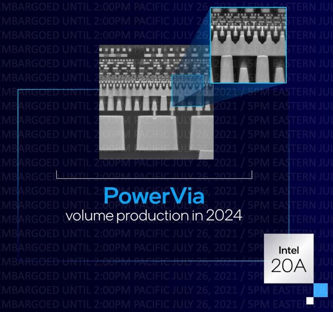
The other arm of Intel’s 20A designs in 2024 is what the company is calling ‘PowerVia’. The concept here pivots the traditional understanding of chip design from a multi-layered cake into a sandwich of sorts.
The manufacturing process of a modern circuit starts the transistor layer, M0, as the smallest layer. Above that, additional metal layers are added at increasing sizes to account for all the wiring needed between the transistors and different parts of the processor (cache, buffers, accelerators). A modern high-performance processor typically has anywhere from 10 to 20 metal layers in its design, with the top layer where the external connections are placed. The chip is then flipped over (known as flip chip) so that the chip can talk to the outside world with those connections on the bottom, and the transistors at the top.
With PowerVias, we now put the transistors in the middle of the design. On one side of the transistors we put the communication wires that allow parts of the chip to talk to each other. On the other side are all the power related connections (along with power gating control). In essence, we moved to a sandwich where the transistors are the filling. This is usually referred to as ‘backside power delivery’ in the industry – PowerVia is Intel’s marketing name.
From a holistic level, we can ascertain that the benefits of this design start with simplifying both the power and the connectivity wires. Typically these have to be designed to ensure there is no signaling interference, and one of the big sources of interference are large power carrying wires, so this takes them out of the equation by putting them on the other side of the chip. It also works the other way – the interference of the interconnected data wires can increase the power delivery resistance, resulting in lost energy and thermals. In this way, PowerVias can help new generations of transistors as drive currents increase by having the power directly there, rather than routed around the connectivity.
There are a couple of hurdles here to mention however. Normally we start manufacturing the transistors first because they are the most difficult and most likely to have defects – if a defect is caught early in the metrology (defect detection in manufacturing), then that can be reported as early in the cycle as possible. By having the transistors in the middle, Intel would now be manufacturing several layers of power first before getting to the tough bit. Now technically these layers of power would be super easy compared to the transistors, and nothing is likely to go wrong, but it is something to consider.
The second hurdle to think about is power management and thermal conductivity. Modern chips are built transistor first into a dozen layers ending with power and connections, and then the chip is flipped, so the power hungry transistors are now at the top of the chip and the thermals can be managed. In a sandwich design, that thermal energy is going to go through whatever ends up on the top of the chip, which is most likely going to be the internal communication wires. Assuming that the thermal increase of these wires doesn’t cause any issues in production or regular use, then perhaps this isn’t so much of an issue, however it is something to consider when heat has to be conducted away from the transistors.
It is worth noting that this ‘backside power delivery’ technology has been in development for a number of years. Across five research papers presented at the VLSI symposium in 2021, imec presented several papers on the technology showing recent advancements when using FinFETs, and in 2019 Arm and imec announced similar technology on an Arm Cortex-A53 built on an equivalent 3nm process in imec’s research facilities. Overall the technology reduces the IR drop on the design, which is becoming increasingly harder to achieve on more advanced process node technologies to drive performance. It will be interesting to see the technology when it is in high volume on high performance processors.
Intel’s Next Generation Packaging: EMIB and Foveros
Alongside the process node advancements, Intel also has to march forward with next-generation packaging technology. The demand for high performance silicon coupled with increasingly difficult process node development has created an environment where processors are no longer a single piece of silicon, relying on multiple smaller (and potentially optimized) chiplets or tiles to be packaged together in a way that benefits performance, power, and the end product.
Single large chips are no longer the smart business decision – they can end up too difficult to make without defects, or the technology to create them isn’t optimized for any one particular feature on the chip. However, dividing a processor up into separate silicon pieces creates additional barriers to moving data around between those pieces – if the data has to transition from being in silicon to being in something else (such as a package or an interposer) then there is a power cost and latency cost to consider. The tradeoff is optimized silicon built for purpose, such as a logic chip made on a logic process, a memory chip made on a memory process, and the smaller chips often have better voltage/frequency characteristics when binning than their larger counterparts. But underpinning all of this is how the chips are put together, and that requires packaging.
Intel’s two main specialist packaging technologies are EMIB and Foveros. Intel explained the future of both in relation to its future node development.
EMIB: Embedded Multi-Die Interconnect Bridge
Intel’s EMIB technology is designed for chip-to-chip connections when laid out on a 2D plane.
The easiest way for two chips on the same substrate to talk to each other is by taking a datapath through the substrate. The substrate is a printed circuit board made of layers of insulated material interspersed with metal layers etched into tracks and traces. Depending on the quality of the substrate, the physical protocol, and the standard being used, it costs a lot of power to transmit data through the substrate, and bandwidth is reduced. But, this is the cheapest option.
The alternative to a substrate is to put both chips onto an interposer. An interposer is a large piece of silicon, big enough for both chips to wholly fit on to, and the chips are bonded directly to the interposer. Similarly there are data paths put into the interposer, but because the data is being moved from silicon to silicon, the loss of power is not as much as a substrate, and the bandwidth can be higher. The downside to this is that the interposer also has to be manufactured (usually on 65nm), the chips involved have to be small enough to fit, and it can be rather expensive. But, the interposer is a good solution, and active interposers (with built in logic for networking) have yet to be fully exploited).
Intel’s EMIB solution is a combination of both interposer and substrate. Rather than taking a large interposer, Intel uses a small slither of silicon and embeds that directly into the substrate, and Intel calls this a bridge. The bridge is effectively two halves with hundreds or thousands of connections each side, and the chips are built to connect to one half of the bridge. Now both chips are connected to that bridge, having the benefit of transferring data through silicon without the restrictions that a large interposer might bring. Intel can embed multiple bridges between two chips if more bandwidth is needed, or multiple bridges for designs using more than two chips. Also, the cost of that bridge is much less than a large interposer.
With those explanations, it sounds like Intel’s EMIB is a win-win. There have been a few limitations to the technology – actually embedding a bridge into a substrate is kind of hard. Intel has spent several years and lots of money trying to perfect the technology for low power operation. On top of this, whenever you are adding multiple elements together, there is an associated yield with that process – even if connecting a chip to a bridge has a 99% yield, doing it with a dozen chips on a single design reduces the overall yield down to 87%, even when starting with known good chips (that have their own yield). When you hear that Intel has been working on bringing this technology to volume, it is these numbers they are trying to improve.
Intel currently has EMIB in the market on several of its products, most noticeably its Stratix FPGA and Agilex FPGA families, but it was also part of its Kaby G line of mobile processors, connecting a Radeon GPU to high-bandwidth memory. Intel has already stated that it is coming to several future products, such as Ponte Vecchio (supercomputer-class graphics), Sapphire Rapids (next generation Xeon enterprise processor), Meteor Lake (2023 consumer processor), and others related to graphics.

Intel's Ponte Vecchio uses EMIB and Foveros
On the roadmap side of EMIB, Intel is reducing the bump pitch over the next few years. When the chips are connected to the bridges embedded in the substrate, they connect across bumps, and the distance between the bumps is known as the pitch – the smaller the bump pitch, the more connections can be made in the same area. This allows the chip to either increase bandwidth, or reduce the bridge size. The first generation EMIB technologies in 2017 were using 55 micron bump pitches, and that still appears to be the case with upcoming Sapphire Rapids (see my comment about the time it has taken Intel to get it right), however Intel is aligning itself with a 45 micron EMIB beyond Sapphire Rapids, leading to a 36 micron EMIB in its third generation. The timescales for these were not disclosed, however post Sapphire Rapids would be Granite Rapids, so that might be where the 45 micron design comes to market.
Foveros: Die to Die Stacking
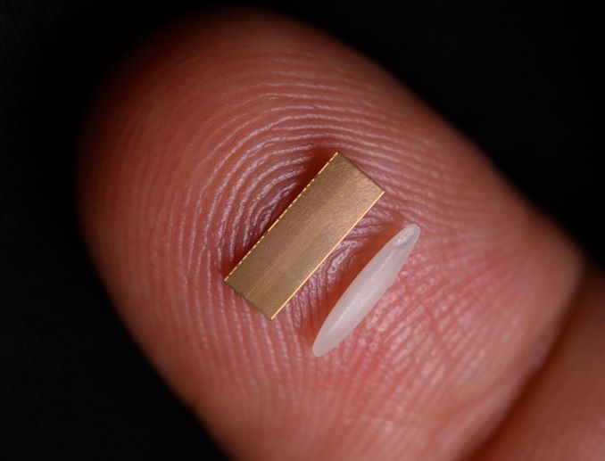
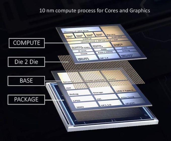
Intel introduced its die-to-die stacking technology in 2019 with Lakefield, a mobile processor designed for low idle power designs. That processor has since been put on End of Life proceedings, but the idea is still integral to the future of Intel’s future product portfolio and foundry offerings.
Intel’s die-to-die stacking is to a large extent very similar to the interposer technology mentioned in the EMIB section. We have one piece of silicon (or more) on top of another. In this instance however, the interposer, or base die, has active circuitry relevant for the full operation of the main compute processors found in the top piece of silicon. While the cores and graphics were on the top die in Lakefield, built on Intel’s 10nm process node, the base die had all the PCIe lanes, USB ports, security, and everything low power related to IO, and was built on a 22FFL low power process node.
So while EMIB technology splitting the silicon to work alongside each other is known as 2D scaling, by placing the silicon on top of each other we have entered a full 3D stacking regime. This comes with some good benefits, especially at scale – data paths are a lot shorter, leading to less power loss due to shorter wires but also better latency. The die-to-die connections are still bonded connections, with the first generation at a 50 micron pitch.
But there are two key limitations here: thermals and power. To avoid problems with thermals, Intel made the base die have very little logic and used a low power process. With power, the issue is enabling the top compute die to have power for its logic – this involves large power through-silicon-vias (TSVs) from the package up through the base die into the top die, and those TSVs carrying power become an issue for localized data signaling due to interference caused by high currents. There is also a desire to scale to smaller bump pitches in future processes, allowing for higher bandwidth connections, requiring more attention to be paid by the power delivery.
The first announcement related to Foveros today is regarding a second generation product. Intel’s 2023 consumer processor, Meteor Lake, has already been described above as using an Intel 4nm compute tile, taking advantage of EUV. Intel is also stating today that it will be using its second generation Foveros technology on the platform, implementing a bump pitch of 36 micron, effectively doubling the connection density over the first generation. The other tile in Meteor Lake has not been disclosed yet (either what it has or what node it is on), however Intel is also stating that Meteor Lake will scale from 5 W to 125 W.
Foveros Omni: Third Generation Foveros
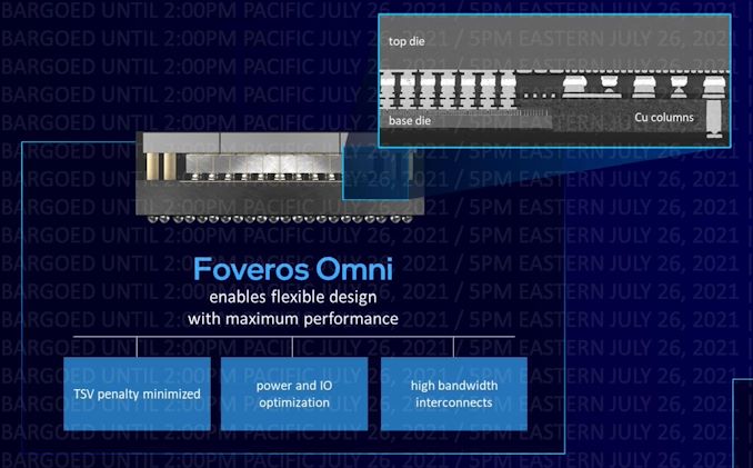
For those that have been following Intel’s packaging technologies closely, then the name ‘ODI’ might be familiar. It stands for Omni-Directional Interconnect, and it was the moniker being floated in previous Intel roadmaps regarding a packaging technology that allows for cantilevered silicon. That is now going to be marketed as Foveros Omni.
This means that the limit of the first generation Foveros which needed a top die smaller than the base die is now removed. The top die can be larger than the base die, or if there are multiple die on each of the levels, they can be connected to any number of other silicon. The goal of Foveros Omni is really to solve the power problem as discussed in the initial section on Foveros – because power carrying TSVs cause a lot of localized interference in signaling, the ideal place to put them would be on the outside of the base die. Foveros Omni is a technology that allows for the top die to overhang from the base die and copper pillars are built from the substrate up to the top die to provide power.
With this technology, if power can be brought in from the edges of the top die, then this method can be used. I did wonder, however, that with large silicon if power would be better fed right up the middle – Intel has stated that Foveros Omni works with split base dies, such that power carrying copper pillars could be placed in the middle of the design if the base die is designed for substrate to be available on that lower layer.
By moving the power TSVs outside the base die, this also allows for a die-to-die bump pitch improvement. Intel is citing 25 microns for Omni, which would be another 50% increase in bump density over second generation Foveros. Intel is expecting Foveros Omni to be ready for volume manufacturing in 2023.
Foveros Direct: Fourth Generation Foveros
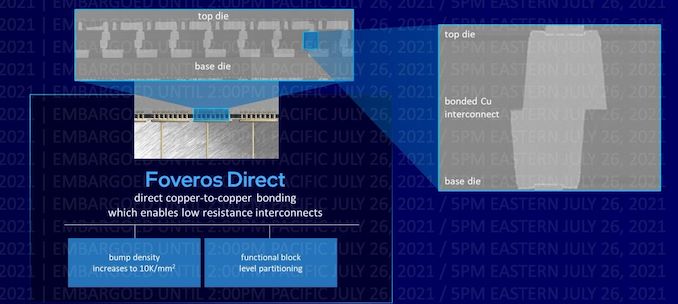
One of the issues with any die-to-die connectivity is the connection itself. In all of these technologies mentioned so far, we’re dealing with microbump bonded connections – small copper pillars with a tin solder cap, which are put together and ‘bonded’ to create the connection. As these technologies are growing copper and the depositing tin solder, it gets difficult to scale them down, plus there is also the power loss of the electronics transferring into the different metals. Foveros Direct gets around this problem, by doing direct copper-to-copper bonding.
Rather than rely on pillars and bumps coming together, the concept of direct silicon-to-silicon connectivity has been researched for a number of years. If one piece of silicon is lined up directly with another, then there is little-to-no need for extra steps to grow copper pillars and such. The issue comes with making sure that all the connections are made, ensuring that both the top die and bottom die are so incredibly flat that nothing can get in the way. Also, the two pieces of silicon have to become one, and are permanently bonded together without any way of coming apart.
Foveros Direct is a technology that helps Intel drive the bump pitch of its die-to-die connections down to 10 micron, a 6x increase in density over Foveros Omni. By enabling flat copper-to-copper connections, bump density is increased, and the use of an all-copper connection means a low resistance connection and power consumption is reduced. Intel has suggested that with Direct, functional die partitioning also becomes easier, and functional blocks could be split across multiple levels as needed.
Technically Foveros Direct as a die-to-die bonding could be considered complimentary to Foveros Omni with the power connections outside the base die – both could be used independently of each other. Direct bonding would make internal power connections easier, but there would still be the issue of interference perhaps, which Omni would take care of.
It should be noted that TSMC has a similar technology, known as Chip-on-Wafer (or Wafer-on-Wafer), with customer products set to come to the market in the coming months using 2-high stacks. TSMC has demonstrated a 12-high stack in mid-2020, however this was a test vehicle for signaling, rather than a product. The issue going up in stacks is still going to be thermals, and what goes into each layer.
Intel predicts that Foveros Direct, like Omni, will be ready for mass volume in 2023.
Customers Customers Customers
As a roadmap announcement today, the focus isn’t so much on the customers but on the technology. Because Intel is moving into a phase where it expects its IFS offerings to compete against the established players, it has to consider its disclosures with respect to both its internal use and any external interest, which is a new concept for the company – at least on this scale compared to its previous foundry efforts.
Intel CEO Pat Gelsinger, in the company’s Q3 financial call last week, was keen to point out that they already have a large hyperscaler customer signed up for their next generation packaging technology, however today there would appear to also be another customer in the mix. Now we assume that Intel’s Foundry Services is talking to 100s of chip companies, big and small, but it doesn’t take much to sign an NDA to start to talk – what will be interesting is when customers start making commitments to using Intel’s facilities, and if any of those are volume orders.
As part of the announcement today, Intel held a little bit back from us, saying that they are saving some of the details specifically for the event that is going on as we publish this piece. All we know is that our draft press release has a big yellow bar that says ‘[customer news]’ on it, right next to Intel’s 20A process node details.
For reference, Intel 20A is a 2024 technology using first generation Gate-All-Around transistors, marketed as RibbonFETs, as well as backside power delivery, marketed as PowerVias. At this time Intel expects to have second/third-generation EMIB available as well as fourth-generation Foveros Direct. So if a customer is already committing to Intel 20A, there’s going to be a lot of potential here.
When the announcement is made, we will update this news article.
To conclude, Intel maintains that these roadmaps will showcase a clear path to process performance leadership* by 2025. It’s a tall order, and the company has to execute better than it has in recent memory - but that’s kind of why the company has rehired a number of former Intel experts and fellows in research, product design, and execution.
*as measured by performance per watt at iso-power
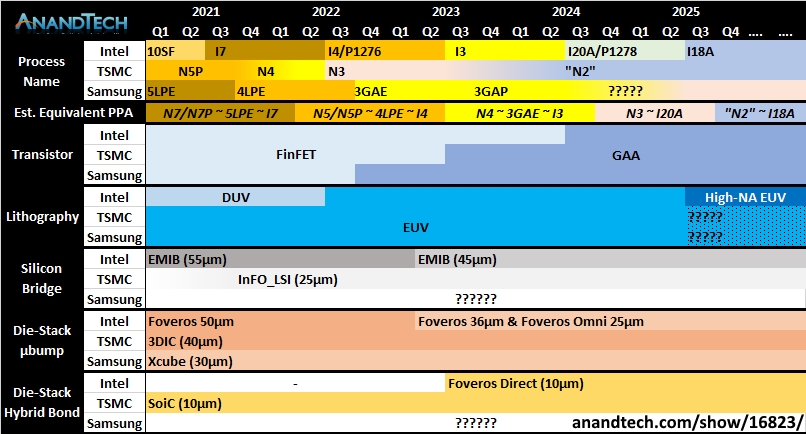
Here's a secondary comparison chart (compared to the one on page one) with all three main foundry offerings listed in each of the main segments that Intel has discussed today.

