Original Link: https://www.anandtech.com/show/4991/arms-cortex-a7-bringing-cheaper-dualcore-more-power-efficient-highend-devices
ARM's Cortex A7: Bringing Cheaper Dual-Core & More Power Efficient High-End Devices
by Anand Lal Shimpi on October 19, 2011 12:31 PM EST- Posted in
- CPUs
- Arm
- Cortex A15
- Smartphones
- Mobile
- Cortex A7
- Tablets
- SoCs
How do you keep increasing performance in a power constrained environment like a smartphone without decreasing battery life? You can design more efficient microarchitectures, but at some point you’ll run out of steam there. You can transition to newer, more power efficient process technologies but even then progress is very difficult to come by. In the past you could rely on either one of these options to deliver lower power consumption, but these days you have to rely on both - and even then it’s potentially not enough. Heterogeneous multiprocessing is another option available - put a bunch of high performance cores alongside some low performance but low power cores and switch between them as necessary.
NVIDIA recently revealed it was doing something similar to this with its upcoming Tegra 3 (Kal-El) SoC. NVIDIA outfitted its next-generation SoC with five CPU cores, although only a maximum of four are visible to the OS. If you’re running light tasks (background checking for email, SMS/MMS, twitter updates while your phone is locked) then a single low power Cortex A9 core services those needs while the higher performance A9s remain power gated. Request more of the OS (e.g. unlock your phone and load a webpage) and the low power A9 goes to sleep and the 4 high performance cores wake up.
While NVIDIA’s solution uses identical cores simply built using different transistors (LP vs. G), the premise doesn’t change if you move to physically different cores. For NVIDIA, ARM didn’t really have a suitable low power core thus it settled on a lower power Cortex A9. Today, ARM is expanding the Cortex family to include a low power core that can either be used by itself or as an ISA-compatible companion core in Cortex A15 based SoCs. It’s called the ARM Cortex A7.
Architecture
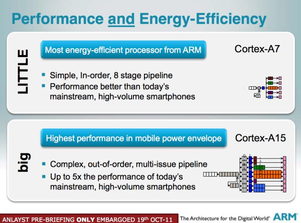
Starting with the Cortex A9, ARM moved to an out-of-order execution core (instructions can be reordered around dependencies for improved parallelism) - a transition that we saw in the x86 space back in the days of the Pentium Pro. The Cortex A15 continues the trend as an OoO core but increases the width of the machine. The Cortex A7 however takes a step back and is another simple in-order core capable of issuing up to two instructions in parallel. This should sound a lot like the Cortex A8, however the A7 is different in a number of areas.
The A8 is a very old design with work originally beginning on the core in 2003. Although ARM offered easily synthesizable versions of the core, in order to hit higher clock speeds you needed to include a lot of custom logic. The custom design requirements on A8 not only lengthened time to market but also increased development costs, limiting the A8’s overall reach. The Cortex A7 on the other hand would have to be fully synthesizable while being able to deliver good performance. ARM could leverage process technology advancements over the past few years to deliver clock speed and competitive power consumption, but it needed a revised architecture to meet the cost and time to market requirements.
The Cortex A7 features an 8-stage integer pipeline and is capable of dual-issue. Unlike the Cortex A8 however, the A7 cannot dual-issue floating point or NEON instructions. There are other instructions that turn the A7 into a single-issue machine as well. The integer execution cluster is quite similar to the Cortex A8, although the FPU is fully pipelined and more compact than its older brother.
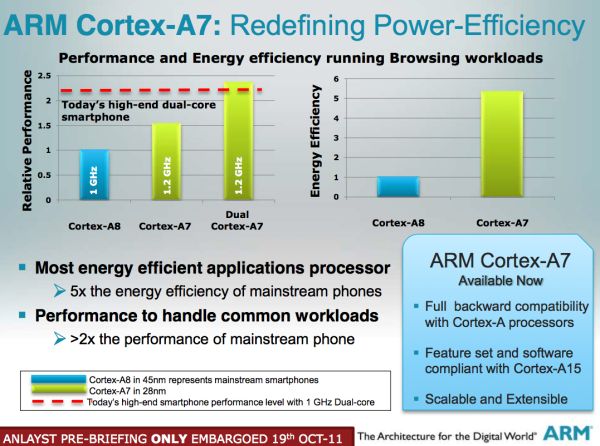
Limiting issue width for more complex instructions helps keep die size in check, which was a definite goal for the core. ARM claims a single Cortex A7 core will measure only 0.5mm2 on a 28nm process. On an equivalent process node ARM expects customers will be able to implement an A7 in 1/3 - 1/2 the die area of a Cortex A8. As a reference, an A9 core uses about the same (if not a little less) die area as an A8 while an A15 is a bit bigger than both.
| Architecture Comparison | |||||||||
| ARM11 | ARM Cortex A7 | ARM Cortex A8 | ARM Cortex A9 | Qualcomm Scorpion | Qualcomm Krait | ||||
| Decode | single-issue | partial dual-issue | 2-wide | 2-wide | 2-wide | 3-wide | |||
| Pipeline Depth | 8 stages | 8 stages | 13 stages | 8 stages | 10 stages | 11 stages | |||
| Out of Order Execution | N | N | N | Y | Partial | Y | |||
| Pipelined FPU | Y | Y | N | Y | Y | Y | |||
| NEON | N/A | Y (64-bit wide) | Y (64-bit wide) | Optional MPE (64-bit wide) | Y (128-bit wide) | Y (128-bit wide) | |||
| Process Technology | 90nm | 40nm/28m | 65nm/45nm | 40nm | 40nm | 28nm | |||
| Typical Clock Speeds | 412MHz | 1.5GHz (28nm) | 600MHz/1GHz | 1.2GHz | 1GHz | 1.5GHz | |||
Despite the limited dual issue capabilities, ARM is hoping for better performance per clock and better overall performance out of the Cortex A7 compared to the Cortex A8. Branch prediction performance is improved partly by using a more modern predictor, and partly because the shallower pipeline lessens the mispredict penalty. The Cortex A7 features better prefetching algorithms to help improve efficiency. ARM also includes a very low latency L2 cache (10 cycles) with its Cortex A7 design, although actual latency can be configured by the partner during implementation.
Note that in decoding bound scenarios, the Cortex A7 will offer the same if not lower performance than a Cortex A8 due to its limited dual-issue capabilities. The mildly useful DMIPS/MHz ratings of ARM’s various cores are below:
| Estimated Core Performance | |||||||||
| ARM11 | ARM Cortex A7 | ARM Cortex A8 | ARM Cortex A9 | Qualcomm Scorpion | Qualcomm Krait | ||||
| DMIPS/MHz | 1.25 | 1.9 | 2.0 | 2.5 | 2.1 | 3.3 | |||
The big news is the Cortex A7 is 100% ISA compatible with the Cortex A15, this includes the new virtualization instructions, integer divide support and 40-bit memory addressing. Any code running on an A15 can run on a Cortex A7, just slower. This is a very important feature as it enables SoC vendors to build chips with both Cortex A7 and Cortex A15 cores, switching between them depending on workload requirements. ARM calls this a big.LITTLE configuration.
big.LITTLE: Heterogeneous ARM MP
The Cortex A15 is going to be a significant step forward in performance for ARM architectures. ARM hopes it will be enough to actually begin to threaten the low end of the x86 space, which gives you an idea of just how powerful these cores are going to be. The A15 will also find its way into smartphones and tablets, ultimately replacing the Cortex A9s used by high-end devices today.
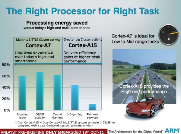
For heavy workloads, the Cortex A15 is expected to be more power efficient than the A9. The core may draw more instantaneous power, but it will do so for a shorter period of time thus allowing the CPU(s) to get to sleep quicker and reducing average power.
As ARM has often argued (particularly against Intel) however, these big out-of-order microprocessor architectures are inefficient at dealing with lightweight mobile workloads. In particular, things like background tasks running on your phone while it’s locked in your pocket simply don’t demand the performance of a Cortex A15. ARM further argues that the power consumed by an A15 running these tasks, even though only for a short period of time, is greater than it would be on a much simpler in-order architecture. This is where the A7 comes into play.
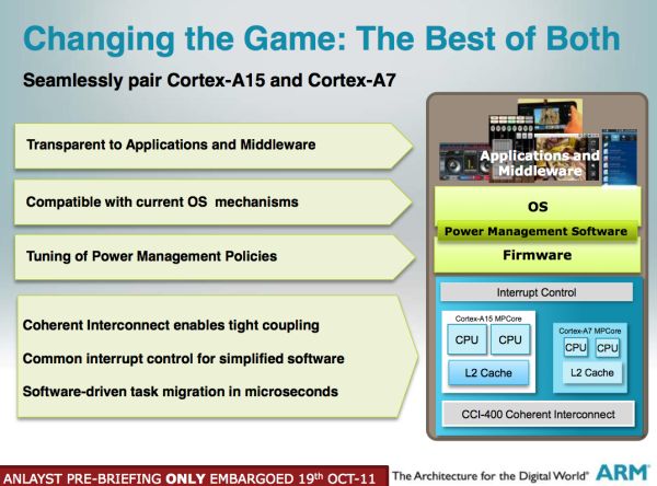
Although the Cortex A7 is fully capable of being used on its own (and it most definitely will be), ARM’s partners are free to integrate Cortex A7 cores alongside Cortex A15 cores in a big.LITTLE (or little.BIG?) configuration.
Since the A7 and A15 are equally capable of executing the same ARM instruction set, any applications running on one core can just as easily be migrated to run on the other. In the example above there are a pair of A15s and a pair of A7s on a single SoC. In this particular configuration, the OS only believes there are two cores in the machine. ARM’s own power management firmware determines which core cluster to activate depending on performance states requested by the OS. If the OS wants a high performance state, ARM returns the A15 cores at a high p-state. If it wants a low performance state, the chip will put the A15s to sleep and schedule everything on the A7s. Cache coherency is guaranteed via the CCI-400 interconnect, so any data invalidated by one core cluster will be reflected in the other cluster’s cache. ARM claims it can switch between core clusters in this configuration in as quick as 20 microseconds.
If everything works the way ARM has described it, a big.LITTLE configuration should be perfectly transparent to the OS (similar to what NVIDIA is promising with Kal-el). ARM did add that SoC vendors are free to expose all cores to the OS if they would like, although doing so would obviously require OS awareness of the different core types.
Core Configurations, Process Technology & Final Words
ARM’s Cortex A7 will be available in 1 - 4 core configurations, both as the primary CPU in an SoC as well as in a big.LITTLE configuration alongside some A15s. ARM expects that we will see some 40nm A7 designs as early as the end of next year for use in low end smartphones (~$100). Most smartphone configurations, even at these price points will likely use dual-core A7 implementations. It’s only in emerging markets that ARM is expecting to see single core Cortex A7 smartphone devices. This is pretty big news as it means that even value smartphones will be dual-core by 2013.
Costs will keep the A7 on 40nm for a while although the cores will be offered at 28nm for integration into A15 designs as well as for even higher performance/lower power implementations.
I have to say that I’m pretty excited about the Cortex A7 announcement across the board. It looks like this core will not only enable much better performance at the value end of the device spectrum but it should bring battery life improvements at the high end as well. Chip architects have argued for years that we were going to see heterogeneous computing as the next phase in the evolution of microprocessors, it’s fascinating to see that we may get the first consumer application of it in ultra mobile devices.


