Original Link: https://www.anandtech.com/show/5365/intels-medfield-atom-z2460-arrive-for-smartphones
Intel's Medfield & Atom Z2460 Arrive for Smartphones: It's Finally Here
by Anand Lal Shimpi on January 10, 2012 8:00 PM ESTIt's here. Intel's first smartphone SoC that you'll actually be able to buy in a device before the end of the year. The platform is called Medfield and Paul Otellini just announced its first device partners.
Medfield starts out as a bonafide mobile SoC. Whereas Moorestown was a "two-chip" solution, Medfield is just one - the Penwell SoC:
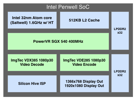
The SoC is only available in a PoP (Package on Package) configuration measuring 12mm x 12mm. Intel wouldn't give out a die size but it did show me a Penwell sample without the stacked DRAM:
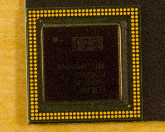
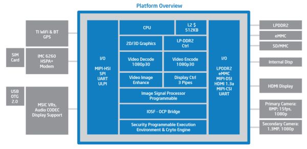
Since I know the measurements of the package I could estimate the dimensions of the silicon itself. My math worked out to be around 62mm^2. That's larger than a Tegra 2-class SoC, but smaller than Tegra 3 or Apple's A5. The diagram of its high level architecture above helps explain why.
There's only a single version of Medfield being announced today: the Intel Atom Z2460. The Z2460 features a single Atom core with a 512KB L2 cache, a PowerVR SGX 540 GPU and a dual-channel LPDDR2 memory interface. In a world where talking about four Cortex A9s and PowerVR SGX 544MP2s isn't uncommon, Medfield starts out almost sounding a bit...tame. But then you see its performance:
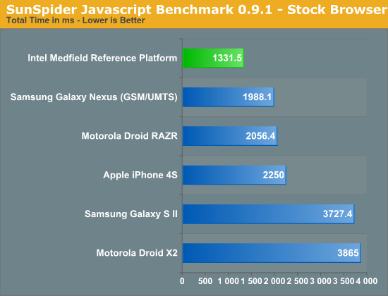
Although running what appears to be a stock Gingerbread browser, Intel's Medfield reference platform posts SunSpider performance better than any other smartphone we've tested - including the Galaxy Nexus running Ice Cream Sandwich. Intel promises that Medfield's performance will scale on ICS as well - the gap should be maintained. We've seen high results from reference designs in the past, but the Medfield platform is a little different as you'll soon see - it's a complete smartphone design that should be representative of handsets that hit the market later this year.
Medfield isn't a one trick pony either, performance is similarly dominating under BrowserMark:
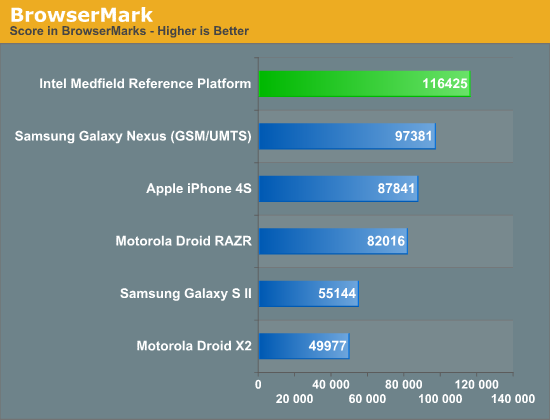
These are tablet-like scores. Here the Galaxy Nexus running ICS comes close, but once again Intel expects that on the same OS Medfield should be faster than any of the currently available SoCs.
I asked Intel where its SunSpider and BrowserMark performance advantages came from, especially considering we've typically only seen huge gains with new browsers and not new SoCs. Their response pointed to a bunch of factors, but one stand out issue was the A9 has a great execution core but seems to be more limited on the memory interface. Atom can support far more outstanding misses in L2 than the Cortex A9, which chokes bandwidth to the processor for anything not already in the L2 cache. This may be one of the reasons why we've never been able to get really high bandwidth numbers out of A9 based SoCs. It's probably safe to assume that things will be different with the Cortex A15, but for now it's little things like this that give Medfield a performance advantage.
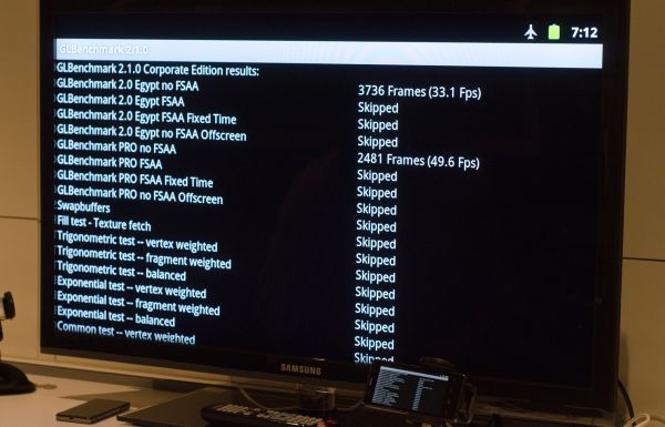
GPU performance is understandably not as impressive. We couldn't get offscreen numbers of GLBenchmark 2.1 but we did get results at the device's native resolution (1024 x 600):
3D performance is better than the OMAP 4460 due to Medfield's 400MHz GPU clock compared to ~300MHz in most OMAP4 devices.
Performance without power considerations is meaningless, especially in the smartphone world. Luckily for Intel, Medfield seems very competitive there as well. Intel provided some power and performance data for Medfield based on its reference platform. I still haven't been able to verify any of this for myself, but I was able to see some power tests run in person on the reference platform and competitive devices.
The Intel provided values are pretty astonishing . Sub 20mW idle, sub 750mW during a call on 3G and although not pictured here, Intel's internal data suggests ~1W power consumption while browsing the web compared to ~1.3W on the iPhone 4S and Galaxy S 2. I've done my own measurements on 4S web browsing and came up with a very similar value.
| Intel Measured Smartphone Power Consumption (Identical Display Brightness) | ||||||
| Standby (3G) | Talk (3G) | Browsing (3G) | Video Playback 720p | |||
| Apple iPhone 4S | ~38mW | ~800mW | ~1.3W | ~500mW | ||
| Intel Medfield Reference | ~18mW | ~700mW | ~1.0W | ~850mW | ||
| Samsung Galaxy S II | ~19mW | ~675mW | ~1.2W | ~650mW | ||
The performance and power data both look great for Medfield. You would think that this data, assuming there's nothing fundamentally wrong, would be enough to convince a handset maker to actually give Intel a shot. You'd be right.
In addition to disclosing Medfield performance data, Intel is also announcing partnerships with both Motorola and Lenovo. The former is a broad, multi-year agreement stating that Motorola plans on creating many devices based on Intel silicon - the first of which will be a smartphone due out before the end of the year. Tablets will follow at some point as well.
Lenovo on the other hand will actually be taking and tweaking Intel's own Medfield reference platform, and releasing it in China in Q2.
All of this is exactly what Intel needed: a start.
The CPU
Medfield is the platform, Penwell is the SoC and the CPU inside Penwell is codenamed Saltwell. It's honestly not much different than the Bonnell core used in the original Atom, although it does have some tweaks for both power and performance.
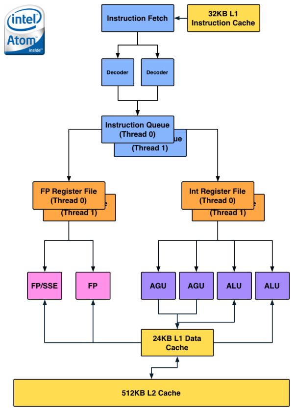
Almost five years ago I wrote a piece on the architecture of Intel's Atom. Luckily (for me, not Intel), Atom's architecture hasn't really changed over the years so you can still look back at that article and have a good idea of what is at the core of Medfield/Penwell. Atom is still a dual-issue, in-order architecture with Hyper Threading support. The integer pipeline is sixteen stages long, significantly deeper than the Cortex A9's. The longer pipeline was introduced to help reduce Atom's power consumption by lengthening some of the decode stages and increasing cache latency to avoid burning through the core's power budget. Atom's architects, similar to those who worked on Nehalem, had the same 2:1 mandate: every new feature added to the processor's design had to deliver at least a 2% increase in performance for every 1% increase in power consumption.
Atom is a very narrow core as the diagram below will show:
There are no dedicated integer multiply or divide units, that's all shared with the FP hardware. Intel duplicated some resources (e.g. register files, queues) to enable Hyper Threading support, but stopped short of increasing execution hardware to drive up efficiency. The tradeoff seems to have worked because Intel is able to deliver performance better than a dual-core Cortex A9 from a single HT enabled core. Intel also lucks out because while Android is very well threaded, not all tasks will continually peg both cores in a dual-core A9 machine. At higher clock speeds (1.5GHz+) and with heavy multi-threaded workloads, it's possible that a dual-core Cortex A9 could outperform (or at least equal) Medfield but I don't believe that's a realistic scenario.
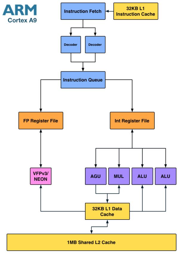
Architecturally the Cortex A9 doesn't look very different from Atom:
Here we see a dedicated integer multiply unit (shared with one of the ALU ports) but only a single port for FP/NEON. It's clear that the difference between Atom and the Cortex A9 isn't as obvious at the high level. Instead it's the lower level architectural decisions that gives Intel a performance advantage.
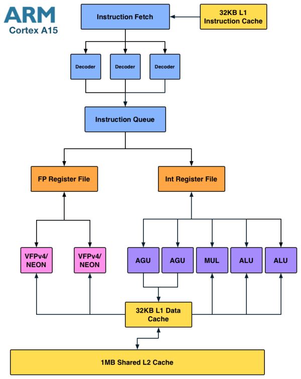
Where Intel is in trouble is if you look at the Cortex A15:
The A15 is a far more modern design, also out of order but much wider than A9. I fully expect that something A15-class can outperform Medfield, especially if the former is in a dual-core configuration. Krait falls under the A15-class umbrella so I believe Medfield has the potential to lose its CPU performance advantage within a couple of quarters.
Enhancements in Saltwell
Although the CPU core is mated to a 512KB L2 cache, there's a separate 256KB low power SRAM that runs on its own voltage plane. This ULP SRAM holds CPU state and data from the L2 cache when the CPU is power gated in the deepest sleep state. The reasoning for the separate voltage plane is simple. Intel's architects found that the minimum voltage for the core was limited by Vmin for the ULP SRAM. By putting the two on separate voltage planes it allowed Intel to bring the CPU core down to a lower minimum power state as Vmin for the L2 is higher than it is for the CPU core itself. The downside to multiple power islands is an increase in die area. Since Medfield is built on Intel's 32nm LP process while the company transitions to 22nm, spending a little more on die area to build more power efficient SoCs isn't such a big deal. Furthermore, Intel is used to building much larger chips, making Medfield's size a relative nonissue for the company.
The die size is actually very telling as it's a larger SoC than a Tegra 2 with two Cortex A9s despite only featuring a single core. Granted the rest of the blocks around the core are different, but it goes to show you that the CPU core itself (or number of cores) isn't the only determination of the die size of an SoC.
The performance tweaks come from the usual learnings that take place over the course of any architecture's lifespan. Some instruction scheduling restrictions have been lifted, memory copy performance is up, branch predictor size increased and some microcode flows run faster on Saltwell now.
Clock Speeds & Turbo
Medfield's CPU core supports several different operating frequencies and power modes. At the lowest level is its C6 state. Here the core and L2 cache are both power gated with their state is saved off in a lower power on-die SRAM. Total power consumption in C6 of the processor island is effectively zero. This isn't anything new, Intel has implemented similar technologies in desktops since 2008 (Nehalem) and notebooks since 2010 (Arrandale).
When the CPU is actually awake and doing something however it has a range of available frequencies: 100MHz all the way up to 1.6GHz in 100MHz increments.
The 1.6GHz state is a burst state and shouldn't be sustained for long periods of time, similar to how Turbo Boost works on Sandy Bridge desktop/notebook CPUs. The default maximum clock speed is 1.3GHz, although just as is the case with Turbo enabled desktop chips, you can expect to see frequencies greater than 1.3GHz on a fairly regular basis.
Power consumption along the curve is all very reasonable:
| Medfield CPU Frequency vs. Power | ||||||
| 100MHz | 600MHz | 1.3GHz | 1.6GHz | |||
| SoC Power Consumption | ~50mW | ~175mW | ~500mW | ~750mW | ||
Since most ARM based SoCs draw somewhere below 1W under full load, these numbers seem to put Medfield in line with its ARM competitors - at least on the CPU side.
It's important to pay attention to the fact that we're dealing with similar clock frequencies to what other Cortex A9 vendors are currently shipping. Any performance advantages will either be due to Medfield boosting up to 1.6GHz for short periods of time, inherently higher IPC and/or a superior cache/memory interface.
The GPU
The PowerVR SGX 540 in Medfield is no different from what you'd get in an OMAP 4460, with the exception that it's clocked a bit higher at 400MHz.
The SGX 540 here is a remnant of Intel's earlier strategy to have Medfield out far sooner than it actually is going to show up on the market. Thankfully Intel has plans to introduce a PowerVR SGX 543MP2 based Medfield successor also before the end of the year.
Video Decode/Encode Support, Silicon Hive ISP
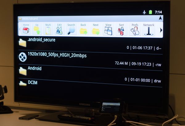
Intel relies on two more IP blocks from Imagination Technologies: the VDX385 and VDE285 for 1080p video decode and encode. Intel claims support for hardware accelerated 1080p30 decode, High Profile. Maximum supported bitrate is apparently up to 50Mbps, although Intel only demonstrated a 20Mbps High Profile stream:
Intel also claims support for 1080p30 video encode.
Medfield's ISP is provided by Intel owned Silicon Hive. The ISP supports cameras ranging from 5MP to 16MP (primary sensor), with the reference design standardizing on an 8MP sensor. Medfield supports burst capture at up to 15 fps (8MP).
The Process
Intel bifurcated its process technology a few years ago, offering both low power and high performance versions of each of its process nodes. Today those process nodes are staggered (45nm LP after high perf 32nm, 32nm LP debuts after high performance 22nm, etc...) however Intel plans on bringing both in lockstep.
Medfield debuts on Intel's 32nm LP process. The only details we have from Intel are that leakage is 10x lower than the lowest on 45nm. Compared to Moorestown, Medfield boasts 43% lower dynamic power or 37% higher frequency at the same power level.
The bigger and more valid comparison is to TSMC's 28nm process, which is what companies like Qualcomm will be using for their next-generation SoCs. It's unclear (and very difficult) to compare different architectures on different processes, but it's likely that Intel's 32nm LP process is more comparable to TSMC's 28nm LP process than it would be to any 4x-nm node.
It is important to note that Intel seems very willing to sacrifice transistor density in order to achieve lower power consumption where possible. I don't believe Intel will have the absolute smallest die sizes in the market, but I also don't believe it's clear what the sweet spot is for mobile SoCs at this point. It's quite likely that Apple's ~120mm^2 target is likely where everyone will eventually end up in the near term.
The Roadmap
Although Medfield is already posting competitive performance numbers, its current competition is roughly a year old. Within the next two quarters we'll see smartphones and tablets shipping based on Qualcomm's Krait. The next-generation Snapdragon platform should be Cortex A15-like in its performance level
Today we have Medfield, a single core Atom paired with a PowerVR SGX 540 built on Intel's 32nm LP process. Before the end of the year we'll see a dual-core Atom based Medfield with some form of a GPU upgrade. I wouldn't be too surprised to see something like a PowerVR SGX 543MP2 at that point either. In tandem Intel will eventually release an entry level SoC designed to go after the more value market. Finally we'll see an Intel Atom based SoC with integrated Intel baseband from its Infineon acquisition - my guess is that'll happen sometime in 2013.
What's Different This Time Around: Google & A Sweet Reference Platform
Intel has been talking about getting into smartphones for a couple of years now, but thus far it hasn't been able to secure a single design or partnership that that resulted in a product actually coming to market. This time around, things are different. The major change? Focus, and Google.
Intel originally had ambitions of enabling its own mobile OS with the help of Nokia (Moblin/MeeGo). Intel also wanted to support Android as well, however its attention was clearly more focused on the Moblin/MeeGo effort. Similar to the wake up call that pushed NVIDIA to focus exclusively on Android, Intel has now done the same.
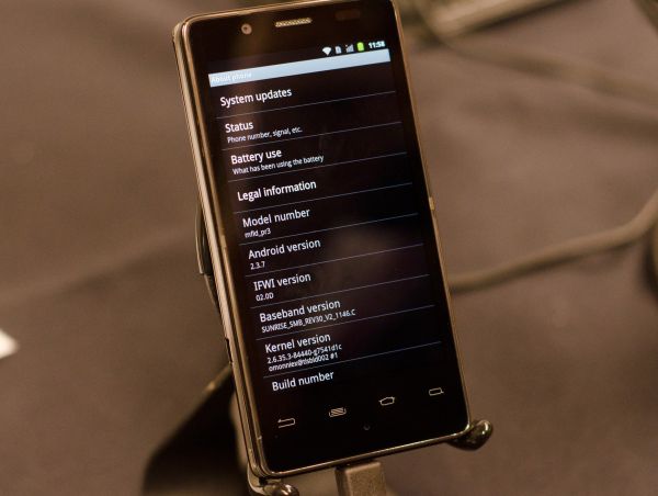
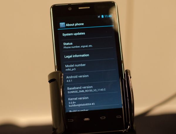
At IDF last year Intel and Google announced a partnership and the intention to bring all future versions of Android, starting with Gingerbread, to x86. Since then Intel has ramped up the software engineering engine, going into the Android source code (Gingerbread, Honeycomb and now ICS) and fixing bugs. Intel's goal is to deliver the most stable version of Android as a result of its efforts. Intel is also submitting its changes upstream to the AOSP, which should help improve the Android experience even on ARM platforms.
Under the leadership of Mike Bell (formerly of Apple and Palm), Intel has also created an extremely polished Medfield reference design. This is the same design shown off at IDF last year (apparently there's an even thinner one floating around somewhere), but what separates it from other reference designs we've seen from SoC vendors is that the Medfield reference platform was designed to be a polished phone that could theoretically be rebranded and resold.
Intel knew the onus was on itself to prove that Medfield, Atom and even just x86 was power efficient enough to be delivered in a compelling form factor with competitive battery life. Paul Otellini gave Mike carte blanche access to any of Intel's resources. Instead of having to work with existing Intel groups, Mike was allowed to assemble his dream team of engineers. The team Mike built is what he felt he needed to not only bring Medfield to market, but also to build the a first class Atom based smartphone.
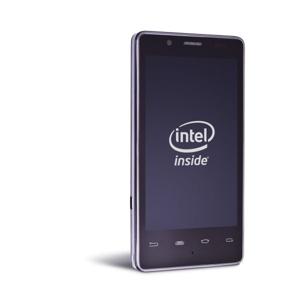
The result is this:
Internally it features Intel's own XMM 6260 HSPA+ modem. Intel claims LTE is on the way although there's no ETA on that.
WiFi in the reference design is provided by TI's 1283 controller. Intel's wireless team does not have a a WiFi solution that's low power enough to work in a smartphone, although after the recent restructuring the team has now been tasked with building an ultra low power solution that can.
The display is a somewhat unusual 1024 x 600 panel, with support for 1080p30 (and 1080i60) output via HDMI. The SoC specs are identical to what I've already discussed: 1.6GHz max CPU clock and a 400MHz GPU clock.
The reference platform is not only smartphone sized, but Intel has built its own qualification labs that mirror those of the carriers to ensure quality and convince its customers of the platform's legitimacy. In essence, Intel has built its own miniature smartphone design and test center.
The Medfield reference platform is available for use by any of Intel's customers, and indeed that's what's already happening. Lenovo's K800 is based on a modified version of Intel's reference platform, and I wouldn't be surprised if more aren't on the way.
All of this sounds a lot like Intel's efforts in the motherboard space over a decade ago where it started providing motherboard manufacturers with reference designs that they could modify if they desired. The effort helped significantly reduce time to market and allowed the motherboard makers to focus more on specializing on what they were good at.
The Medfield reference platform is designed to do the very same for smartphones. Intel wants to provide its partners with a well designed, stable smartphone platform. If they choose to use it, they can shave off a significant amount of development time and spend more of their time on software or simply bring a good reference phone to market in a quick fashion. I'm not entirely sure I've seen many players in the Android space that are actually all that great at software development, but Intel believes anything that shortens time to market will be appreciated.
I asked Intel if it has any plans to offer the reference platform unlocked, direct to customers. Unfortunately the answer at this point is still no. I suspect that Intel is more interested in building its customer base rather than circumventing it.
ARM Compatibility: Binary Translation
Similar to Apple's move from PowerPC to x86, Intel finds itself in a difficult position with bringing Atom to Android. The OS isn't an issue as it has already been ported to x86 and all further releases will be available in both ARM and x86 flavors. The bigger problem is application compatibility.
There's already support for targeting both ARM and x86 architectures in the Android NDK so anything developed going forward should be ok so long as the developer is aware of x86.
Obviously the first party apps already work on x86, but what about those in the Market?
By default all Android apps run in a VM and are thus processor architecture agnostic. As long as the apps are calling Android libraries that aren't native ARM there, once again, shouldn't be a problem. Where Intel will have a problem is with apps that do call native libraries or apps that are ARM native (e.g. virtually anything CPU intensive like a 3D game).
Intel believes that roughly 75% of all Android apps in the Market don't feature any native ARM code. The remaining 25% are the issue. The presumption is that eventually this will be a non-issue (described above), but what do users of the first x86 Android phones do? Two words: binary translation.
Intel isn't disclosing much about the solution, but by intercepting ARM binaries and translating ARM code to x86 code on the fly during execution Intel is hoping to achieve ~90% app compatibility at launch. Binary translation is typically noticeably slower than running native code, although Intel is unsurprisingly optimistic about the experience on Android. I'm still very skeptical about the overall experience but we'll have to wait and see for ourselves.
Final Words
Intel finally did it. After almost five years of talking about getting into mobile phone form factors, Intel went out and built a reference platform that proved what they've been saying was possible all along. Furthermore, Intel also finally landed a couple of partners who are willing to show their support by incorporating Medfield into their product portfolio. The releases are still a few months away at the earliest (possibly even longer for Motorola) but it's much better news than Intel has ever reported before in this space.
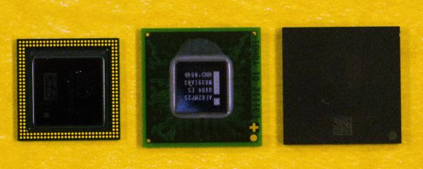
Medfield (left 1) vs. Moorestown (right 2)
The partnerships aren't out of pity either: Medfield is fast. I firmly believe had it been released a year ago it would have dominated the Android smartphone market from the very start. Even today it appears to deliver better CPU performance than anything on the market, despite only having a single core. GPU performance is still not as fast as what's in the A5 but it's competitive with much of the competition today, and I fully expect the dual-core version of Medfield to rectify this problem.
Based on the data Intel shared with us as well, the x86 power problem appears to be a myth - at least when it comes to Medfield. I'm still not fully convinced until we're able to test a Medfield based phone ourselves, but power efficiency at the chip level doesn't seem to be a problem.
Medfield and the Atom Z2460 are a solid starting point. Intel finally has a chip that they can deliver to the market and partners to carry it in. Intel also built a very impressive reference platform that could lead to some very interesting disruptions in the market.
While I'd like to say that Intel's Medfield team can now breathe a sigh of relief, their work is far from over - especially with more competitive ARM based SoCs showing up later this year. I'm really interested to see where this goes in the next 12 months...

