Original Link: https://www.anandtech.com/show/6787/nvidia-tegra-4-architecture-deep-dive-plus-tegra-4i-phoenix-hands-on
NVIDIA Tegra 4 Architecture Deep Dive, Plus Tegra 4i, Icera i500 & Phoenix Hands On
by Anand Lal Shimpi & Brian Klug on February 24, 2013 3:00 PM EST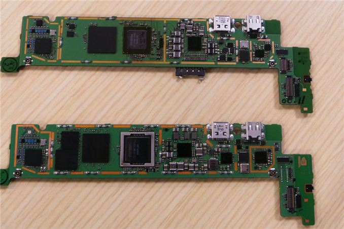
Ever since NVIDIA arrived on the SoC scene, it has done a great job of introducing its ultra mobile SoCs. Tegra 2 and 3 were both introduced with a healthy amount of detail and the sort of collateral we expect to see from any PC silicon vendor. While the rest of the mobile space is slowly playing catchup, NVIDIA continued the trend with its Tegra 4 and Tegra 4i architecture disclosure.
Since Tegra 4i is a bit further out, much of NVIDIA’s focus for today’s disclosure focused on its flagship Tegra 4 SoC due to begin shipping in Q2 of this year along with the NVIDIA i500 baseband. At a high level you’re looking at a quad-core ARM Cortex A15 (plus fifth A15 companion core) and a 72-core GeForce GPU. To understand Tegra 4 at a lower level, we’ll dive into the individual blocks beginning, as usual with the CPU.
ARM’s Cortex A15 and Power Consumption
Tegra 4’s CPU complex sees a significant improvement over Tegra 3. Despite being an ARM architecture licensee, NVIDIA once again licensed a complete processor from ARM rather than designing its own core. I do fundamentally believe that NVIDIA will go the full custom route eventually (see: Project Denver), but that’s a goal that will take time to come to fruition.
In the case of Tegra 4, NVIDIA chose to license ARM’s Cortex A15 - the only vanilla ARM core presently offered that can deliver higher performance than a Cortex A9.
Samsung recently disclosed details about its Cortex A15 implementation compared to the Cortex A7, a similarly performing but more power efficient alternative to the A9. In its ISSCC paper on the topic Samsung noted that the Cortex A15 offered up to 3x the performance of the Cortex A7, at 4x the area and 6x the power consumption. It’s a tremendous performance advantage for sure, but it comes at a great cost to area and power consumption. The area side isn’t as important as NVIDIA has to eat that cost, but power consumption is a valid concern.
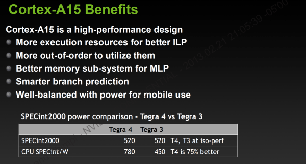
To ease fears about power consumption, NVIDIA provided the following data:
The table above is a bit confusing so let me explain. In the first row NVIDIA is showing that it has configured the Tegra 3 and 4 platforms to deliver the same SPECint_base 2000 performance. SPECint is a well respected CPU benchmark that stresses everything from the CPU core to the memory interface. The int at the end of the name implies that we’re looking at purely single threaded integer performance.
The second row shows us the SPECint per watt of the Tegra 3/4 CPU subsystem, when running at the frequencies required to deliver a SPECint score of 520. By itself this doesn’t tell us a whole lot, but we can use this data to get some actual power numbers.
At the same performance level, Tegra 4 operates at 40% lower power than Tegra 3. The comparison is unfortunately not quite apples to apples as we’re artificially limiting Tegra 4’s peak clock speed, while running Tegra 3 at its highest, most power hungry state. The clocks in question are 1.6GHz for Tegra 3 and 825MHz for Tegra 4. Running at lower clocks allows you to run at a lower voltage, which results in much lower power consumption. In other words, NVIDIA’s comparison is useful but skewed in favor of Tegra 4.
What this data does tell us however is exactly how NVIDIA plans on getting Tegra 4 into a phone: by aggressively limiting frequency. If a Cortex A15 at 825MHz delivers identical performance at a lower power compared to a 40nm Cortex A9 at 1.6GHz, it’s likely possible to deliver a marginal performance boost without breaking the power bank.
That 825MHz mark ends up being an important number, because that’s where the fifth companion Cortex A15 tops out at. I suspect that in a phone configuration NVIDIA might keep everything running on the companion core for as long as possible, which would address my fears about typical power consumption in a phone. Peak power consumption is still going to be a problem I think.
Cortex A15 Architecture
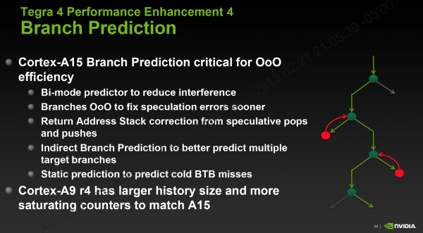
I want to go deeper into ARM’s Cortex A15 but I’ll have to save that for another time. At a high level you’re looking at a much deeper, much wider architecture than the Cortex A9. The integer pipeline is significantly deeper (15 stages vs. 9 stages), however branch prediction has been improved considerably to hopefully offset the difference.
The front end is 50% wider and has double the instruction fetch bandwidth of the Cortex A9, which helps increase instruction level parallelism. In order to capitalize on the 3-wide machine, ARM dramatically increased the size of the reorder buffer and all associated data structures within the machine. While the Cortex A9 could keep around 32 - 40 decoded instructions in its reorder buffer, Cortex A15 can hold 128 - an increase of up to 4x. The larger ROB alone gives you a good idea of the magnitude of difference between the Cortex A9 and A15. While the former was a natural evolution over the Cortex A8, ARM’s Cortex A15 is really a leap forward both in performance and power consumption - clearly aimed at something much more than just smartphones.
Getting to the execution core, A15 continues the trend of being considerably wider than A9. There are more execution ports and more execution units, all of which help to increase ILP/single threaded performance. ARM went to multiple, independent issue queues in order to keep frequencies high. Each issue queue can accept up to three instructions and all issue queues can dispatch in parallel.
The A15 can execute instructions out of order like the A9, however its abilities grow quite a bit. All FP/NEON instructions had to be executed in-order on Cortex A9, but they can now be executed OoO in the A15. Despite the beefier OoO execution engine, the Cortex A15 can’t reorder all memory operations (independent loads can be executed out of order, but stores can’t be completed ahead of loads).
The Cortex A15 moves back to an integrated L2 cache structure, rather than a separate IP block as was the case with the Cortex A9. L1 and L2 cache latencies remain largely unchanged, although I do believe A15 does see a 1 - 2 cycle penalty over A9 in a few cases. The level 2 TLB and other data structures grow in size considerably in order to feed the hungrier machine.
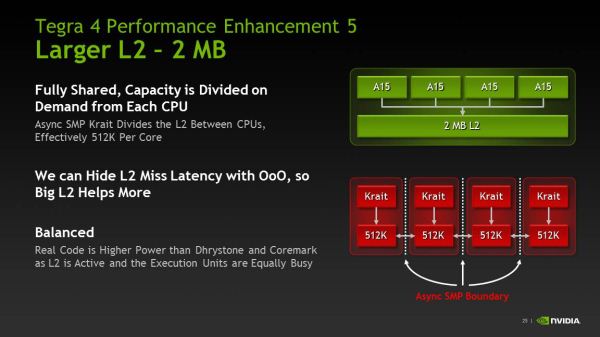
Although the L1 caches remain the same size as NVIDIA’s Cortex A9 (32KB I + 32KB D), the the L2 cache grows to 2MB. The 2MB L2 is shared by all four cores (the companion core has its own private 512KB L2), and any individual core can occupy up to the entire 2MB space on its own. Alternatively, all four cores can evenly share and access the large L2.
The Cortex A9 r4p1
Although we just call ARM’s previous architecture by its Cortex A9 name, there have been multiple revisions to the A9 architecture since its introduction. Tegra 2 implemented Cortex A9 r1p1, while Tegra 3 used r2p9. With Tegra 4i, NVIDIA moved to the absolute latest version of the Cortex A9 core: r4p1.
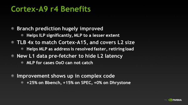
There are some significant changes to the Cortex A9 in r4p1. The GHB, L2 TLB and BTAC all grew by 4x and are now sized equally between the A9 and A15 implementations (16K predictors, 512 entries and 4096 entries, respectively). These changes help improve branch prediction accuracy, which further increases IPC on an already very efficient design.
The A9 r4p1 also has an enhanced data prefetching engine, including a small L1 prefetcher and dedicated hardware for the cache preload instruction.
NVIDIA claims a 15% increase in SPECint_base for the Cortex A9 r4p1 vs. r2p9, which is pretty impressive. Combined with the 2.3GHz max frequency, Tegra 4i’s CPU performance should be a healthy improvement over what we have in Tegra 3 today.
Tegra 4 Clock Speeds
Each of the four primary Cortex A15s is driven off the same voltage and frequency plane, although each core can be power gated individually. This is similar to how Intel designs its processors, but at odds with Qualcomm’s independent voltage/frequency planes.
NVIDIA does a good job of binning its SoCs, and the same will continue with Tegra 4. All four cores are capable of running at up to 1.9GHz, although NVIDIA claims we may see configurations with even higher single core boost frequencies (or even lower max frequencies, similar to Tegra 3). As I already mentioned, the fifth Cortex A15 runs at somewhere between 700 and 800MHz.
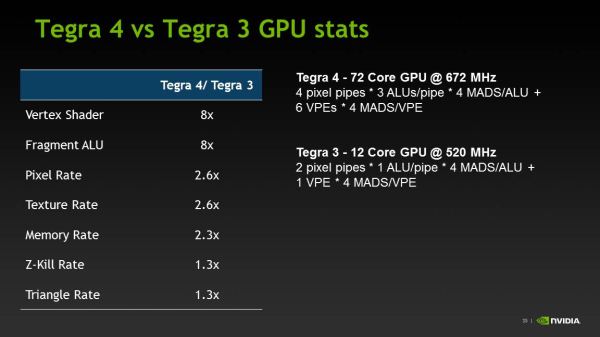
The Tegra 4 GPU operates at up to 672MHz, up from the 520MHz max in Tegra 3.
Round Two, Still Quad-Core
I have to give NVIDIA credit, back when it introduced Tegra 3 I assumed its 4+1 architecture was surely a gimmick and to be very short lived. I remember asking NVIDIA’s Phil Carmack point blank at MWC 2012 whether or not NVIDIA would standardize on four cores for future SoCs. While I expected a typical PR response, Phil surprised me with an astounding yes. NVIDIA was committed to quad-core designs going forward. I still didn’t believe it, but here we are in 2013 with NVIDIA’s high-end and mainstream roadmaps both exclusively featuring quad-core SoCs. NVIDIA remained true to its word, and the more I think about it, the more the approach makes sense.
In the PC industry we learned that there’s no real downside to quad-core as long as you can power gate individual cores, and turbo up to higher frequencies when fewer than four cores are active, there’s no real tradeoff other than cost. You get good multithreaded performance when you need it, and single threaded performance doesn’t suffer. Tegra 3 complicated things because it was on an older, more power hungry process when Qualcomm introduced its first Krait parts. Tegra 4 on the other hand comes to market on the absolute latest and greatest 28nm HPL process from TSMC. And like Tegra 3, each Cortex A15 core in Tegra 4 can be independently power gated.
Like most of the evolution in the mobile space, NVIDIA skipped the silly transitional period between dual and many core and just ended up exactly where it knows the story ends. Heavily threaded apps are still rare on mobile OSes, but with each core independently power gated the user shouldn’t pay a penalty for them being there as long as NVIDIA and the device vendor don’t configure the DFVS tables improperly.
The downside is cost, not to the end user, but to NVIDIA. Economically, NVIDIA was able to make Tegra 3 work for itself with a die size somewhere around 80mm^2. The move to 28nm allowed NVIDIA to increase transistor count, without straying from that die size. Tegra 4 is a bit larger than Tegra 3, but it’s still somewhere in that 80mm^2 range.
Wafer costs for 28nm HPL are undoubtedly higher than 40nm LPG at TSMC, not to mention any differences in yield between T3 and T4, so without a doubt Tegra 4 will cost NVIDIA more than Tegra 3. All of that being said however, NVIDIA still seems to take a conservative approach to die sizes in mobile, which gives it the flexibility to significantly undercut Qualcomm in costs to OEMs. I do believe this was a key part of NVIDIA’s success last year with Tegra 3 ending up in both the Nexus 7 and Microsoft’s Surface RT. Long term, simply selling your SoCs for less than the competition isn’t a path to market dominance, but being able to do so helps buy NVIDIA time while it gathers the remaining missing pieces of the mobile platform (integrated baseband, RF front end, WiFi, etc...). Tegra 4 isn’t the sort of drive the industry forward type of silicon we’re used to seeing from NVIDIA, but it’s sized appropriately given NVIDIA’s position in the market. From a business standpoint, NVIDIA is making the right decisions to ensure the Tegra business at least has a chance of succeeding.
The GPU
Tegra 4 features an evolved GPU core compared to Tegra 3. The architecture retains a fixed division between pixel and vertex shader hardware, making it the only modern mobile GPU architecture not to adopt a unified shader model.
I already described a lot of what makes the Tegra 4 GPU different in our original article on the topic. The diagram below gives you an idea of how the pixel and vertex shader hardware grew over the past 3 generations:
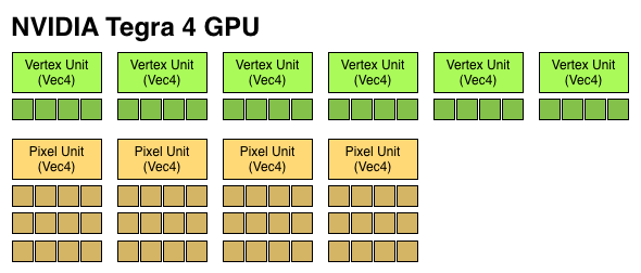
We finally have a competitive GPU architecture from NVIDIA. It’s hardly industry leading in terms of specs, but there’s a good amount of the 80mm^2 die dedicated towards pixel and vertex shading hardware. There's also a new L2 texture cache that helps improve overall bandwidth efficiency.
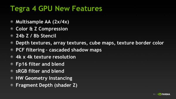
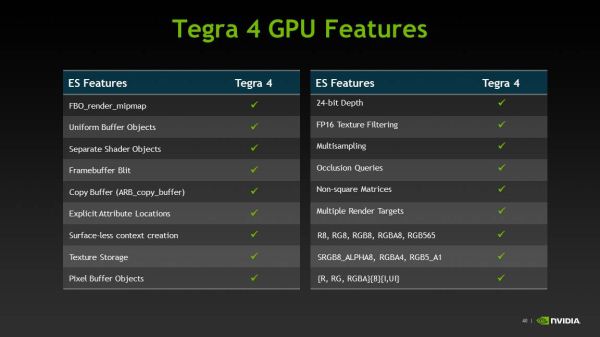
The big omission here is the lack of full OpenGL ES 3.0 support. NVIDIA’s pixel shader hardware remains FP24, while the ES 3.0 spec requires full FP32 support for both pixel and vertex shaders. NVIDIA also lacks ETC and FP texture support, although some features of ES 3.0 are implemented (e.g. Multiple Render Targets).
| Mobile SoC GPU Comparison | |||||||||||||||
| GeForce ULP (2012) | PowerVR SGX 543MP2 | PowerVR SGX 543MP4 | PowerVR SGX 544MP3 | PowerVR SGX 554MP4 | GeForce ULP (2013) | ||||||||||
| Used In | Tegra 3 | A5 | A5X | Exynos 5 Octa | A6X | Tegra 4 | |||||||||
| SIMD Name | core | USSE2 | USSE2 | USSE2 | USSE2 | core | |||||||||
| # of SIMDs | 3 | 8 | 16 | 12 | 32 | 18 | |||||||||
| MADs per SIMD | 4 | 4 | 4 | 4 | 4 | 4 | |||||||||
| Total MADs | 12 | 32 | 64 | 48 | 128 | 72 | |||||||||
| GFLOPS @ Shipping Frequency | 12.4 GFLOPS | 16.0 GFLOPS | 32.0 GFLOPS | 51.1 GFLOPS | 71.6 GFLOPS | 74.8 GFLOPS | |||||||||
For users today, the lack of OpenGL ES 3.0 support likely doesn’t matter - but it’ll matter more in a year or two when game developers start using OpenGL ES 3.0. NVIDIA is fully capable of building an OpenGL ES 3.0 enabled GPU, and I suspect the resistance here boils down to wanting to win performance comparisons today without making die size any larger than it needs to be. Remembering back to the earlier discussion about NVIDIA’s cost position in the market, this decision makes sense from NVIDIA’s stance although it’s not great for the industry as a whole.
Tegra 4i retains the same base GPU architecture as Tegra 4, but dramatically cuts down on hardware. NVIDIA goes from 4 down to 3 vertex units, and moves to two larger pixel shader units (increasing the ratio of compute to texture hardware in the T4i GPU). The max T4i GPU clock drops a bit down to 660MHz, but that still gives it substantially more performance than NVIDIA’s Tegra 3.
Memory Interface
The first three generations of Tegra SoCs had an embarrassingly small amount of memory bandwidth, at least compared to Apple, Samsung and Qualcomm. Admittedly, Samsung and Qualcomm were late adopters of a dual-channel memory interface, but they still got there much quicker than NVIDIA did.
With Tegra 4, complaints about memory bandwidth can finally be thrown out the window. The Tegra 4 SoC features two 32-bit LPDDR3 memory interfaces, bringing it up to par with the competition. The current max data rate supported by Tegra 4’s memory interfaces is 1866MHz, but that may go up in the future.
Tegra 4 won’t ship in a PoP (package-on-package) configuration and will have to be paired with external DRAM. This will limit Tegra 4 to larger devices, but it should still be able to fit in a phone.
Unfortunately, Tegra 4i only has a single channel LPDDR3 memory interface. Tegra 4i on the other hand will be available in PoP as well as discrete configurations. The PoP configuration may top out at LPDDR3-1600, while the discrete version can scale up to 1866MHz and beyond.
Tegra 4 Performance
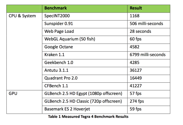
NVIDIA shared a bit of performance data generated from a 1.9GHz Tegra 4 reference tablet. CPU performance is understandably higher than anything we’ve seen from anything ARM or Atom x86 based thus far:
On the GPU front NVIDIA claims to offer performance competitive with Apple’s iPad 4, which is quite impressive considering how far behind NVIDIA had been over the previous two generations.
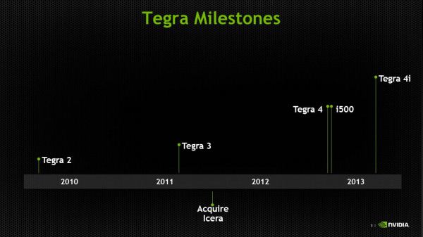
It basically goes without saying, but Tegra 4i, formerly Grey, is primarily a story about the modem. About halfway through 2011, NVIDIA acquired Icera, a player in the handset cellular baseband market who had managed to fit a software-defined radio into the power budget for a mobile device. NVIDIA clearly recognized the importance of being able to deliver an SoC with an integrated modem, and after the Icera acquisition, and later Grey’s appearance on the roadmap, it just became a matter of when that would happen. NVIDIA executed pretty quickly, it turns out, and the fruits of that work manifest themselves in two products — Icera’s standalone i500 and Tegra 4i which contains the same i500 IP block, minus USB interfaces and a different memory subsystem.
Icera was an interesting player in the baseband space because their architecture was that of a software defined radio on the digital baseband side. The reality is that nobody is either fully software defined or burned out to ASIC (hardware), but rather somewhere inbetween. For example, Qualcomm is a combination of software and hardware, though it’s never been entirely clear what functional blocks are ASIC and which other blocks are software, though I’ve been told this is often a matter of whatever is most advantageous for power and what gets re-used most. That said, Icera’s implementation is the furthest towards being pure software defined of anyone, with the entire digital baseband being just one big platform to run their own software atop. There’s an external transceiver which does downconversion, but after that it’s pure software. The question has always been how Icera could afford to build a power competitive platform with an entirely software designed stack, and the clue lies in their choice of 28 HPM instead of LP or HPL silicon for i500 and 4i. Icera designs to a high performance process, then turns off blocks when they’re not in use, rather than make a larger SoC that’s lower leakage. The result is that NVIDIA claims a 40% smaller die for i500 than MDM9x15.
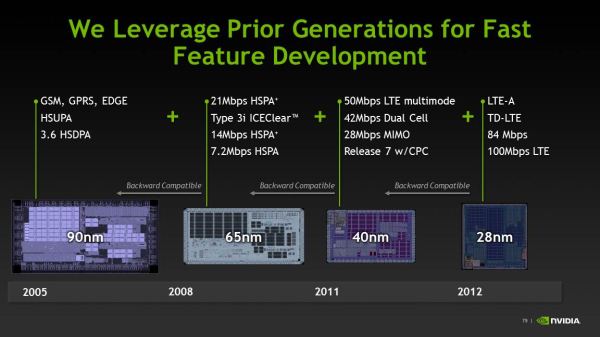
Icera has maintained the same software platform across its modem portfolio, each time taking advantage of increased processing performance afforded by faster silicon to include more air interfaces and capabilities. The result is an interesting advantage when it comes to operator certification — they can make a compelling case for each new version being close to the previous one, since they run the same PHY and protocol stack entirely in software.
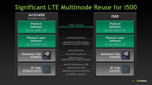
In the case of i500, it runs the exact same multimode modem software as the i4xx series, just with increased DXP support for 15 and 20 MHz channel bandwidths on LTE.
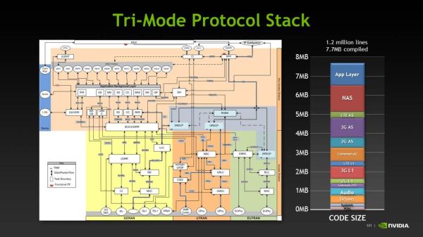
The entire stack ends up being 1.2 million lines of C and DXP code, with a total size of 7.7 MB compiled. NVIDIA gave a great breakdown of the protocol stack as well.
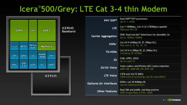
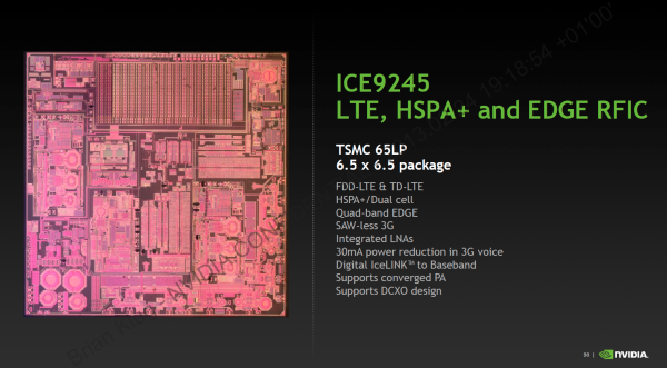
The real name for Icera i500 is ICE9045, and it is paired with a ICE9245 transceiver. ICE9045 is built on 28nm HPM as I mentioned before, and ICE9245 remains 65nm TSMC LP CMOS process which is RF friendly. ICE9045 supports basically all the 3GPP air interfaces, as mentioned in the earlier announcement piece. There’s up to Category 3 LTE on the baseband at launch, with Category 4 in the future. For WCDMA, up to Category 24 (42 Mbps) (dual carrier with 64QAM), and interestingly enough the same Category 18 16 QAM with 2x2 MIMO (28 Mbps) as earlier implemented in Icera 450, and an optional future upgrade to Category 28 64 QAM with 2x2 MIMO (84 Mbps). Of course there’s also TD-SCDMA, GSM/EDGE, full support for voice including AMR-WB and VoLTE/IMS. In addition to 2x2 MIMO the ICE9045 can also do 4x4 MIMO on LTE with a second ICE9245 transceiver.
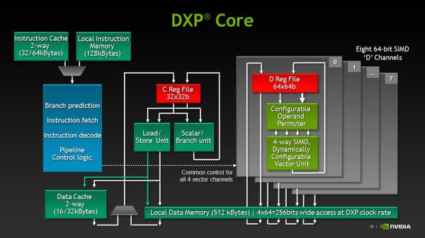
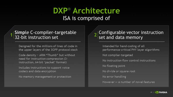
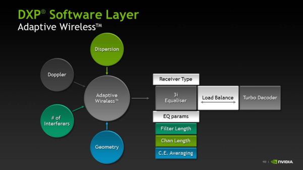
NVIDIA broke down the ICE9045 functionally, which consists of two large DXP units and one smaller DXP unit which runs the rest of the software and management stack. The two larger DXP units run at up to 1.3 GHz. The Icera instruction set consists of two different fundamental sets. Icera refers to these as the “C” and “D” side, with C being rather obvious. The C side is unsurprisingly a C-complier targeted version of the 3GPP protocol stack, and manages the higher level functions of the modem above physical interface, and is a scalar machine. In the block diagram, the C side runs on DXP1, the D side runs on the larger beefier DXP0 and DXP2 machines.
The D side is a proprietary assembly language vector instruction set that runs the physical layer of the modem, this is a combination of specific libraries that really make up the magic and give the Icera platform its reconfigurability. NVIDIA gave an excellent breakdown of the data paths inside both sides. It turns out that in an LTE configuration one core does all the inverse FFTs and MIMO matrix math, the second core does rate matching and decoding. The ultimate goal is to have each of the cores processing around the same equal workload, and since it’s software these tasks can be shuffled in-between to get the i500 running each core at the lowest possible frequency and voltage. Each of the cores can also be individually power collapsed.
On the transceiver side we have ICE9245 which is again TSMC 65nm LP CMOS. This talks over a digital interface to the baseband, and increases the number of primary RX ports from 6 to 8. All filtering and channelization is onboard the ISP. The goal is to keep all the A2D and D2A on the transceiver and away from the baseband. NVIDIA hasn’t quite given me the frequency breakdown for their low band, high band, and super high band, but you can figure it out just by looking. There’s also diversity ports for the same set of bands. All these ports are created equal and can handle 20 MHz LTE, in addition to inter-band and intra-band CA.
The big question is how well Icera’s i500 will stack up against the MDM9x15s and MDM9x25s of the world. Icera believes its ability to switch between four fundamentally different receiver types on the fly and dedicate processing to different functions based on the cellular geometry at the moment offers it an advantage in the long run.
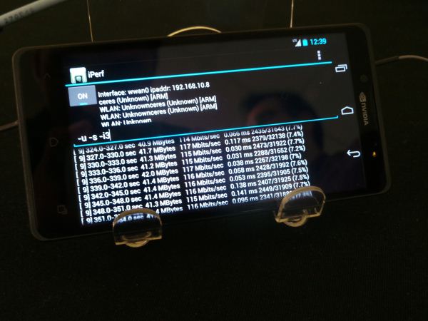
NVIDIA demonstrated a Phoenix with Tegra 4i cabled up to a base station emulator doing full Category 3 LTE at 100 Mbps nice and steady. I asked whether they could go any higher to demonstrate the headroom in the current i500 architecture for upgrading to Category 4 and was shown just short of 120 Mbps on the two week old Tegra 4i silicon.
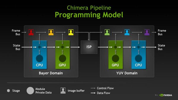
NVIDIA has upped its ISP game with Tegra 4, and includes the same ISP in both Tegra 4 and 4i, which they’ve dubbed Chimera. This new ISP includes a number of features which were already demonstrated at CES, but NVIDIA went into greater detail.
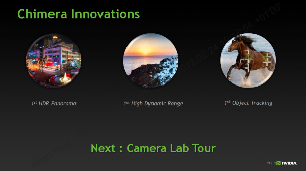
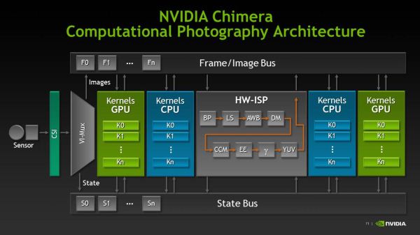
NVIDIA’s major new feature with Tegra 4 is inclusion of new APIs which leverage the GPU to enable computational camera features In addition to the traditional ISP pipeline. To begin, NVIDIA has made their own enhancements in the imaging chain which leverage this GPU-assisted architecture that sits atop the normal ISP. They’ve outlined a few features which work atop this — HDR panorama, HDR stills, and real time object tracking. The end result is that Chimera is one part programming model and APIs for future development efforts by third parties, another part first party software that NVIDIA will distribute for integration in OEM cameras which includes the HDR features and object tracking.
Chimera allows developers to build blocks around the traditional ISP data flow and get to manipulate either bayer image data or YUV space image data on the CPU or GPU using their own framework. There are still a lot of details to come about the programming model and how this will be exploited, but there clearly is space here for NVIDIA to try and make a case for their GPU being useful for image processing. At the same time, the elephant in the room is OpenCL (and its current absence on Tegra 4) and what direction the industry will take that to leverage GPU compute for some computational photography processing.
The novel new feature of note is something I was skeptical about upon seeing at CES — single frame HDR video. The traditional route for HDR video capture is to capture at twice the framerate of the intended output video, for example for 720p30 video with a two-frame HDR, that would mean capture at 720p60 with two different exposures. What NVIDIA does is a bit different. Instead of capturing two exposures and combining them after capture, NVIDIA has found a way to drive selected CMOS sensors (both IMX135 from Sony and AR0833 from Aptina have been called out specifically, but there are more) in some special fashion, and recombine interleaved high and low exposure images (the +1 stop, –1 stop) image into one equivalent frame. This is all done on the GPU using the same Chimera pipeline blocks, but with NVIDIA’s own algorithm. The results are actually pretty impressive, NVIDIA claims 3 stops of dynamic range (~24 dB), and no recombination artifacts.
Previous demonstrations of HDR video capture on a few other platform have had halos around moving elements because of the issues associated with taking two temporally different frames and recombining them. With NVIDIA’s HDR video capture I saw no halos even on very fast moving objects, with the same quality of HDR.
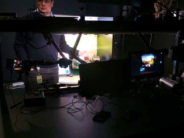
NVIDIA also demonstrated their panorama capture which includes HDR as well, using a GigaPan Epic 100. Admittedly a better demo might be hand held to demonstrate how well the ISP is able to compensate for change in perspective from the tablet moving around in the hand, the resulting image was the same quality of HDR as the still however. I also saw object tracking which essentially is face tracking (and thus AE / AF assist to that subject) but taken to arbitrary subjects. Paint a box around the object you want to track, and the camera will perform feature extraction and machine learn a model around the object. Rotating around complex geometries seemed to work decently well — the model learns slowly so slow movements can be accommodated, faster moving subjects might not be object tracked.
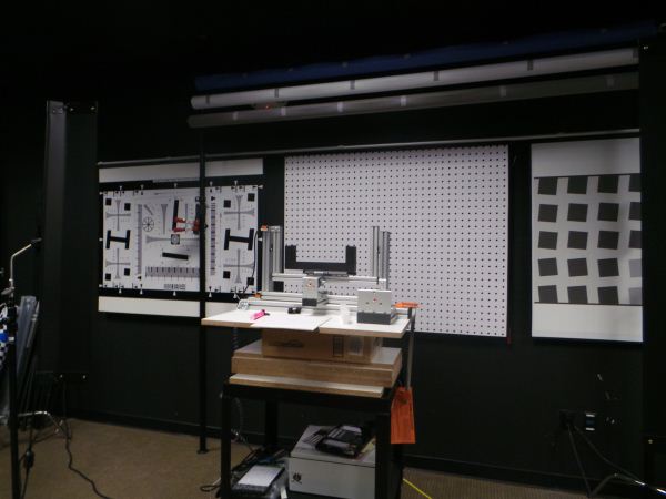
I also got a chance to tour NVIDIA’s camera tuning labs, where they characterize smartphone CMOSes for handset markers, and work with them on tuning their ISP and imaging experience. I saw one calibration room with many different scenes, and then another room with large test charts, and two sets of standard test scenes in lightboxes. The ever-familiar GMB color checker card and ISO12233 charts were everywhere as well.
Silicon makers almost always put together a reference design of their own for both testing their hardware, optimizing software stack, and generally having something to build to. Increasingly we’ve seen these vendors then take that reference design and do something with it beyond just having it for their own internal use — after all, if you’ve built and qualified a device, it makes sense to do something with it. While NVIDIA isn’t going to sell the FFRD directly, it’s a platform they can quickly hand off to OEMs wanting to implement a smartphone-platform with Tegra 4 or 4i relatively quickly.
To that end, NVIDIA has crafted Phoenix, which is their very own FFRD (Form Factor Reference Design) for both Tegra 4 and 4i versions. The high level specifications are what you’d expect for something from this current generation, with a 5-inch 1080p display, LTE, relatively thin profile, and of course a Tegra 4 SoC inside.
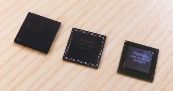
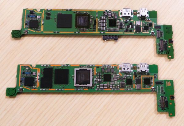
There are actually three different versions of the Phoenix — one in a version with Tegra 4, Tegra 4i without PoP (an external DRAM package), and a Tegra 4i version with PoP memory. All of them have the same PCB geometry inside, just a different SoC, and in the case of the Tegra 4 version, an external Icera i500 modem. NVIDIA showed us an image of their Tegra 4 Phoenix PCB, and in addition the Tegra 4i non PoP and Tegra 4 PCBs in the flesh. The Tegra 4 version has to include both Icera i500 and a MCP DRAM plus NAND of its own adjacent to it, right next to the DRAM for the Tegra 4. On the Tegra 4i version there’s simply unused space in the region occupied by those packages.
Glancing at the Tegra 4i package, we can also get Grey’s actual internal codename, which isn’t T30 series or T40 but rather T8A. The rest of the platform is basically what you’d expect for a modern device, and the PCB follows the rather typical L shaped design that’s common right now across the entire segment.
NVIDIA also showed a Tegra 4i based version of the Phoenix playing a version of Riptide 2 at 1080p with even more graphical assets (real time lighting, shadows, and improved water simulation) enabled over the previous version of Riptide optimized for Tegra 3.
I didn’t get too much time to play with the Phoenix – like any reference design from any of the players in this space it’s more of a function over form piece of equipment for developers or the silicon vendor themselves to get easy access to the insides – but superficially it’s the right kind of stuff for a smartphone right now.
Final Words
NVIDIA’s Tegra 4 is a significant step forward in both CPU and GPU performance. Although Tegra 3 was decent in both areas, Tegra 4 really moves things forward. ARM’s Cortex A15 is an excellent performer, although that performance comes at a high power cost. In a tablet, as we’ve already seen with Google’s Nexus 10, the power consumption associated with the Cortex A15 core is manageable. If NVIDIA’s data is to be believed however, Tegra 4 can get into a smartphone just by aggressively controlling frequencies. At reduced frequencies, Tegra 4 can draw less power than Tegra 3 but with no performance advantage. NVIDIA could then scale up performance (and power) to offer an improvement over Tegra 3. The real question at that point is whether or not Qualcomm’s Krait 300/400 designs offer better efficiency at these intermediate points on the performance/power curve. We’ll be able to find out for sure later this year when both Tegra 4 and Snapdragon 600/800 based devices are shipping.
Icera i500 looks like an interesting competitor in the modem space, which presently is dominated by Qualcomm. More competition is always good, and before the NVIDIA acquisition Icera was on the up and up with impressive performance and interesting SDR architecture. In addition the integration into NVIDIA's own SoC seems to have taken place pretty quickly, and we had the opportunity to see it in the flesh doing over 100 Mbps on a test box.
On the imaging side NVIDIA's Chimera ISP architecutre looks intriguing, though it is obvious that NVIDIA is trying to craft a compelling story for leveraging the GPU. What we did see of HDR video capture and assist looks better than some of the other solutions out there, and object tracking does make for a compelling demo even if it requires user training.
NVIDIA’s biggest advantage hasn’t been architecture, but rather being in the right design wins. Without a doubt, the Nexus 7 and Surface RT were significant wins for NVIDIA last year and they really helped ensure a successful year for NVIDIA’s Tegra business. Whether or not NVIDIA will be able to guarantee similarly key design wins with Tegra 4 remains to be seen. The architecture looks good enough on paper, now it’s just up to NVIDIA’s sales teams to get it into the right devices.

