Original Link: https://www.anandtech.com/show/8362/amds-big-bet-on-arm-powered-servers-a1100-revealed
AMD’s Big Bet on ARM Powered Servers: Opteron A1100 Revealed
by Stephen Barrett on August 11, 2014 12:00 PM EST- Posted in
- IT Computing
- AMD
- Arm
- Opteron
- SoCs
- server
- Enterprise CPUs
- Opteron A1100
It has been a full seven months since AMD released detailed information about its Opteron A1100 server CPU, and twenty two months since announcement. Today, at the Hot Chips conference in Cupertino, CA, AMD revealed the final pieces about its ARM powered server strategy headlining the A1100.
The Case for Low Power Server CPUs
Before we discuss the new Opteron A1100 details, let us review the background of why AMD designed an ARM powered CPU. It all comes down to the devices and services we now take for granted: cell phones, tablets, cloud storage, and cloud services. AMD presented a slide about a year ago that summed it up nicely.
The amount of internet users is growing by 8 to 12% every year. Apple, Google, Microsoft, Facebook, you-name-it, all invest huge sums of money into server farms to provide the services we have come to rely on. This trend gains more and more momentum as software companies like Microsoft try to emulate the success of Apple and Google by selling hardware (Apple) and providing free services (Google) that are ad-supported.
Building the infrastructure to support all these devices and users is a massive undertaking. Typically, companies buy traditional high powered servers (read: Intel Xeon) and partition their computing power up between many tasks as needed. However, this isn’t always the best strategy. For IO tasks, you are always bottlenecked by something other than the CPU, so there is not a reason to throw high cost high power CPUs at the problem. For webserver tasks, response time is paramount. However, with the huge number of users connecting, webservers have become an ‘embarrassingly parallel’ problem you can address with multi core CPUs - as long as there is enough muscle behind each CPU.
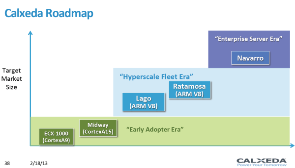
The ‘enough muscle’ issue has hindered previous low power high density webserver attempts. When we tested the Calxeda ARM compute cluster, there were only certain edge cases where it was more efficient than a dual core Xeon server running virtual machines. Calxeda themselves admitted that their processors, utilizing ARM Cortex A9s, were in the early adopter phase of ARM powered webservers. Calxeda stated it wouldn’t be until ARMv8 (where virtualization is supported) and Cortex A57 that ARM based servers would ‘cross the chasm’ and enter the mainstream.
With the Opteron A1100, AMD skipped the early adopter phase and chose something with a higher chance of initial success.
Meet the A1100: CPUs and IO
There are three types of ARM licenses: POP, processor, and architecture. A POP license stands for Processor Optimization Pack and provides the licensee with everything they need to send a chip to the fab. A processor license provides the details of an ARM core like Cortex A9 so you can implement it into your own SoC, but you are not allowed to customize it. Finally, there is the ultimate license, an architecture license. An architecture license provides all details of ARM instruction set (ISA) and CPU implementation so a licensee can implement their own custom CPU core using the ARM ISA however they see fit. AMD is a processor and architecture licensee. If AMD decides it can be competitive by shipping an SoC with an ARM designed CPU (processor license), they can do so without the effort designing their own ARM ISA CPU. If AMD wants to differentiate itself with a custom designed CPU using the ARM ISA, AMD can use its architecture license to do that, similar to Qualcomm’s Krait CPU cores. AMD has decided to do both. Today we discuss its processor license.
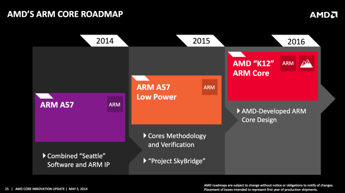
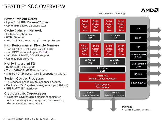
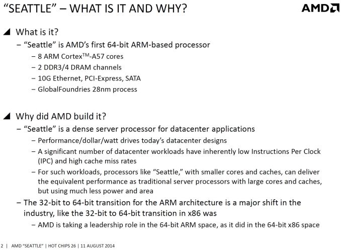
AMD’s first SoC containing an ARM CPU is code named Seattle, the Opteron A1100. Seattle features no less than eight 64-bit ARMv8 ISA, Cortex A57 cores. Depending on availability, this could be the first Cortex A57 CPU to hit any market, not just the server market. AMD will follow up in 2015 with a lower power version that is pin compatible with another x86 CPU, both of which are part of Project Skybridge. In 2016 AMD will leverage its architecture license and ship K12, a fully custom CPU design using the ARMv8 ISA.
Each pair of Cortex A57s in the A1100 shares a 1MB L2 cache (totaling to 4MB of L2), and they all roll up to a shared 8MB L3 cache. To address the server market, all caches are ECC protected except for the L1 instruction cache, which is parity protected instead. Instruction cache protection is not quite as important (invalid instruction just means a pipeline stall). AMD utilizes ARM bus interfaces and debugging support throughout the design. The Cortex A57 also implements cryptography extensions that are quoted by ARM to accelerate things like https by 3-10x over previous ARM designs.
The SoC has a dual channel (2x64-bit) DDR3/4 interface to up to 128GB of 1866MHz memory. Just like the caches, the memory path also supports ECC of the single-bit error correct / double-bit error detect variety. Registered (RDIMM), unregistered (UDIMM), and small-outline (SODIMM) memory modules are support by the A1100 SoC, but actual motherboards will likely support only one type of memory. The same goes for DDR3 vs. DDR4.
As the A1100 is a SoC, it integrates IO directly into the single chip instead of relying on an off-chip IO hub. Integrated components include 8 SATA 3 (6Gb/s) ports, two 10 Gbit Ethernet (10GBASE-KR) ports, one 10/100/1000 Ethernet port, 8 lanes of Gen3 PCI-Express (supporting 8x, 4x/4x, and 4x/2x/2x), I2C, SPI, and UART. The inclusion of this breadth of storage IO (8 SATA3 ports) along with the 2x10 Gbit Ethernet is particularly interesting as it gives us hints of how AMD will position the Opteron A1100 on the market. More on this later.
AMD’s Special Sauce: A1100’s Co-Processors
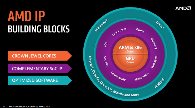
This year, AMD has answered some critics of their business by describing their plans to regain a differentiated position on the market. One of the key slides AMD used to described its position showed ARM, GPU, and x86 cores at the center surrounded by complementary IP.
AMD’s argument is it is uniquely positioned as the only chip company with powerful graphics, ARM and x86 CPU designs, a server heritage including security and fabric (thanks SeaMicro), as well as extensive chip packaging, motherboard and server design expertise.
The complementary IP AMD brings to the A1100 is two Co-Processors. The Cryptographic CoProcessor (CCP) and the System Control Processor (SCP).
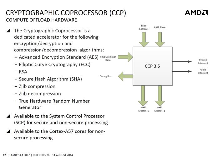
While the Cortex A57s include cryptographic instructions courtesy of the ARMv8 ISA, there are times when a server has significant cryptographic load and it is better to offload that to a coprocessor than service it directly on the CPU core. Cryptographic transactions such as https are well suited for the CPU core as they require low latency and the overhead to offload the work often negates the acceleration the coprocessor provides. However, cryptographic transactions such as archive compression/decompression and large data set encryption/decryption can benefit tremendously.
Utilizing the coprocessor requires operating system awareness to redirect cryptography functions to the dedicated hardware instead of doing them with the general purpose hardware. For example, requesting a random number from the OS would ideally fetch it from the CCP. AMD has already committed an update to the Linux 3.14 kernel to support this.
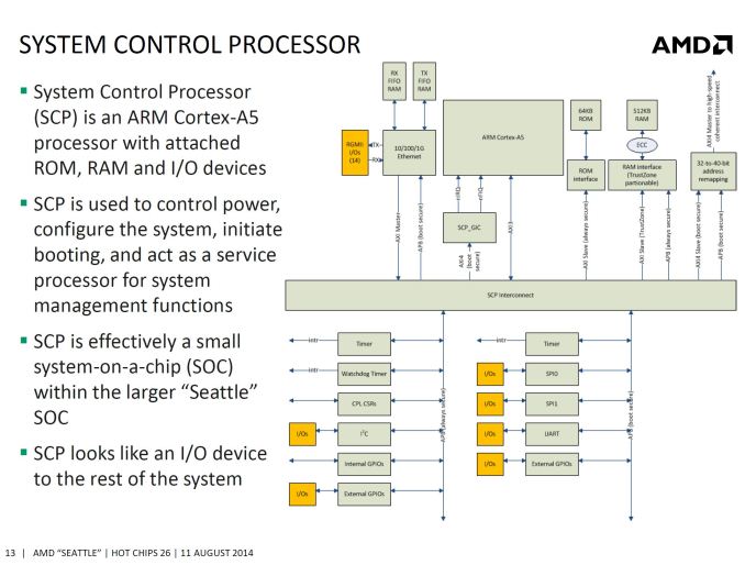
The SCP is based around an ARM Cortex-A5 processor and is effectively an SoC itself inside the A1100 SoC. The rest of the A1100 communicates to the SCP as if it is an IO device. This seems weird, but the isolation is by design. There are two reasons for this: Out-of-band management, and secure processing with ARM TrustZone technology.
Out-of-band management is a technique used in industry for servicing and diagnosing deployed systems regardless of the state of its normal operation or ‘in-band’ components. The SCP has its own dedicated 10/100/100 Ethernet connection, RAM, ROM, and IO connectivity. Connecting from a management interface, a user can read and configure motherboard devices like temperature sensors, power supplies, and fans completely independent from the rest of the A1100 SoC’s activities. Since the SCP is also core to the boot process, server administrators can also reset servers remotely.
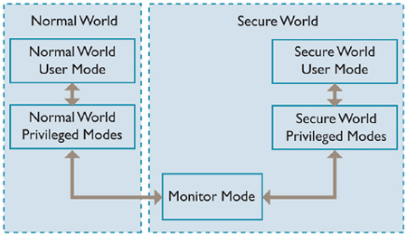
One of the other reasons the SCP exists it to implement ARM's TrustZone technology. AMD announced two years ago they would be partnering with ARM to implement TrustZone technology into future CPUs, and this is the first server CPU to receive the feature. This processor is actually already present in AMD’s x86s APUs. To recap, TrustZone is an ARM technology providing a ‘secure world’ inside the SoC. Programming routines requiring utmost security, like digital rights management, can execute inside the SCP and are protected from unauthorized access from the ‘normal world’. These features are typically found in consumer devices, as certain applications like Netflix require a secure processing path to play HD content. AMD likely reused their TrustZone processor design from consumer APUs to implement the SCP, and it will be interesting to see how server software takes advantage of it.
Reference Design and Final Words
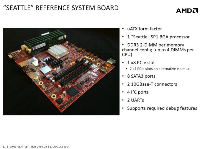
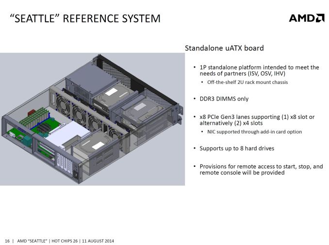
With the A1100, AMD is providing system integrators with a reference design µATX motherboard and 2U server rack. These will demonstrate SoC power delivery, IO and boot configuration, as well as SCP connectivity to integrators to utilize in their own designs.
Interestingly, despite the considerable horsepower contained inside the Opteron A1100 compared to previous non-AMD Cortex A9 server designs, AMD's reference server is clearly not specifically targeting web server applications. The reference design is not computationally dense as it only has one 8-core CPU node in a 2U chassis. The design is targeting storage servers with slots for 8 hard drives.
AMD’s presentation mentions a focus on datacenters where IO connectivity and low power consumption are more important than CPU horsepower. AMD certainly has plenty of server experience and will be well positioned to attack this market with this differentiated product. However, I could not shake the feeling AMD was missing an opportunity in micro severs by not targeting the web server application market with a more processor dense reference design. In fact, digging through our own content on the A1100, I found a quote from Anand saying “AMD sees huge demand in the memcached space, cold storage servers and Apache web front ends. The offer is pretty simple: take cost savings on the CPU front and pour it into more DRAM.” I agree with AMD, the A1100 is well suited for datacenter applications- but we only see one incarnation of that with the storage server reference design.
With the acquisition of SeaMicro adding fabric to AMDs long list of expertise, it is surprising to not see a micro server design that connects dozens of these processors together. Calxeda’s Boston Virdis server is exactly that, and our own conclusions stated that the design has huge promise if it was only a bit faster.
Perhaps it is due to excitement about this CPU that I am looking for a more innovative reference server design. All in all, that is not a bad position to be in. Perhaps it is enough to even convince micro sever companies to buy their CPU from AMD instead of designing their own. One thing is for sure, it will be interesting to watch the server market evolve over the next few years. It might not happen, but there could be a day when using your phone to post to Facebook is serviced end-to-end by ARM CPUs.


